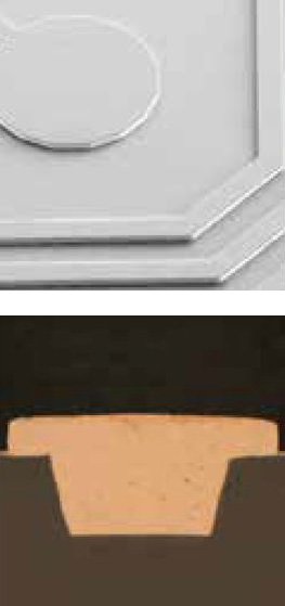
Top: Plating fine lines, Cu pads; bottom: Microvia filling, CD < 20 µm
Berlin, 30 August, 2018: Atotech today announced its participation at this year’s SEMICON Taiwan Show, held from September 5 to 7, 2018, in the Taipei Nangang Exhibition Center Hall 1 in Taipei, Taiwan. The Atotech team can be found at booth J2340 and at the SiP Global Summit where Dr. Ralf Schmidt, R&D Manager Semiconductor at Atotech Group, will exemplify the company’s answer for enhanced reliability of sub 5 µm L/S RDL for 5G.
“Next generation devices for FOWLP require the reduction of the RDL pitch to 1×1 µm or less. This leads to an increased importance of the mechanical properties. Recent findings point out the importance of the formation of a proper composite with the subjacent substrate, i.e. polyimide (PI). The composite formation can strongly improve the mechanical properties and, thus, the reliability of the Cu lines,” states Ralf.
In his presentation on Thursday, September 6, 2018, from 3:45 pm to 4:15 pm, Ralf will discuss the different solutions to promote the formation of a proper composite material consisting of Cu RDL lines and PI, especially with respect to their influence on mechanical properties as well as their suitability for potential 5G applications. The combination of high purity Cu deposits and strong composite formations with the substrate is considered to be a key parameter for future sub 5 µm L/S multilayer RDL technologies.
The company also announced a special product feature on Spherolyte® UF3, a new wet chemical process solution for next generation RDLs in FOWLP, and MultiPlate®, the company’s new production tool for the simultaneous copper deposition for embedded power chips, at booth number J2340.
Spherolyte® UF3
This product allows for fine line RDL plating and microvia filling in one process. Advantages include the low internal stress of less than 20 MPa and the low incorporation level of additives which enables high purity Cu deposits. Spherolyte® UF3 also reduces Cu line breakages after thermal cycle testing.
MultiPlate® for power ICs
MultiPlate® for power ICs was developed for the simultaneous copper deposition for embedding power chips and backside metallization. The Atotech tool allows for plating on 150, 200 and 300 mm wafers including Taiko thin wafers and panel sizes of up to 600 x 600 mm. The dual side metallization process minimizes warpage and enables high deposition uniformity at high plating speeds. This leads to a process cost reduction of up to 26 percent, and reduces the number of process steps by 25 percent, as compared to sequential processing.