Berlin, October 19, 2023 MKS Instruments, Inc. (NASDAQ: MKS), a global provider of enabling technologies that transform our world, today announced that its strategic brands ESI (Laser Systems) and Atotech (process chemicals, equipment, software, and services) will present their combined product offering of leading manufacturing solutions for printed circuit boards and package substrate manufacturing at the upcoming 24th Taiwan Circuit Board Industry International Exhibition (TPCA Show 2023), and the 18th International Microsystems, Packaging, Assembly and Circuit Technology Conference (IMPACT 2023), to be held from October 25th to 27th, 2023 at Taipei Nangang Exhibition Center.
By combining leading capabilities in lasers, optics, motion, process chemistry, and equipment, MKS is best positioned to Optimize the InterconnectSM, a significant enabling point for next-generation advanced electronics that represent the next frontier for miniaturization and complexity. The Optimize the InterconnectSM philosophy highlights the company’s unique position in supporting the development of next-generation advanced PCB and package substrate manufacturing solutions for its customers and partners. “We are committed to enabling new technologies and increasingly smaller feature sizes by combining MKS’ ESI laser drilling technologies with MKS’ Atotech chemistry and plating equipment,” stated Harald Ahnert, VP and GM of Chemistry.”
The company’s combined expertise and know-how across lasers, materials processing, and equipment technology provides numerous opportunities to facilitate collaboration, innovation, and continual ground-breaking solutions for its customers. “We recently installed new systems and process technology in one of our global technology centers to drive the production of next-generation package substrates and provide customers and OEMs alike quicker development cycles for new products and materials enabling high-end SAP technology that require <5/5 µm lines and spaces,” added Harald.
Another example of MKS’ contributions to innovation is the company’s progress in flex, advanced HDI or substrate-like PCBs. Here our customer offering ranges from a comprehensive combination of optimized laser drilling and process chemistries to PCB manufacturing equipment. Customers benefit from the company’s unique one-stop-shop destination for pre-treatment, via formation, plating, and final finishing with quick turn-around times that don’t require an interruption in production, which enables our customers to deliver better yields, productivity, and performance. “For substrate-like PCBs, we are working with the industry to enable next generation mSAP technology,” said Harald Ahnert, VP and GM of Chemistry.
Experts from both brands will be available and ready to discuss latest industry trends and challenges at TPCA Show booth N-718 on the 4th floor of the Nangang Exhibition Hall 1. The dedicated onsite team will introduce new product combinations, including printed circuit board production equipment (wet-to-wet process equipment, laser systems and auxiliary equipment), chemistry, software, and related services.
On the chemistry side, for surface treatment our highlights include EcoFlash® S300, a new differential etching solution suitable for advanced IC substrates and Novabond® EX-S2, our new high-tech adhesion promoter for ultra-fine lines and high-speed applications. For metallization our highlights include Printoganth® MV TP2, a highly capable electroless copper process specifically designed for SAP fine line applications, and our even more enhanced Printoganth® MV TP3 process enabling super thin Cu deposits for fine lines down to 2/2 µm L/S which you want to ideally combine with Cupraganth® MV our new and revolutionary copper-based activation system. For electrolytic copper plating, we are highlighting our new insoluble reverse pulse plating solution for inclusion-free IC substrate core through hole filling for high aspect ratio, Inpulse® 2THF2, and our production proven InPro® SAP3 process for BMV filling with best uniformity at high current densities. For conformal high hole density IC substrate core plating we are promoting Cuprapulse® IN, our new solution for excellent uniformity for high hole density boards.
For final finishing our highlights range from OSP solution OS-Tech® SIT 2, a new generation corrosion-free gold process for ENIG, ENEPIG, and EPAG to new type of immersion tin processes for flex PCBs, as well as for thick tin plating of µ-LED, IC substrates, or solder depot plating.
On the laser equipment side, promotions include the latest Capstone™ (UV Laser for Flex PCBs) and Geode™ (CO2 laser for HDI and package substrate applications) capabilities.
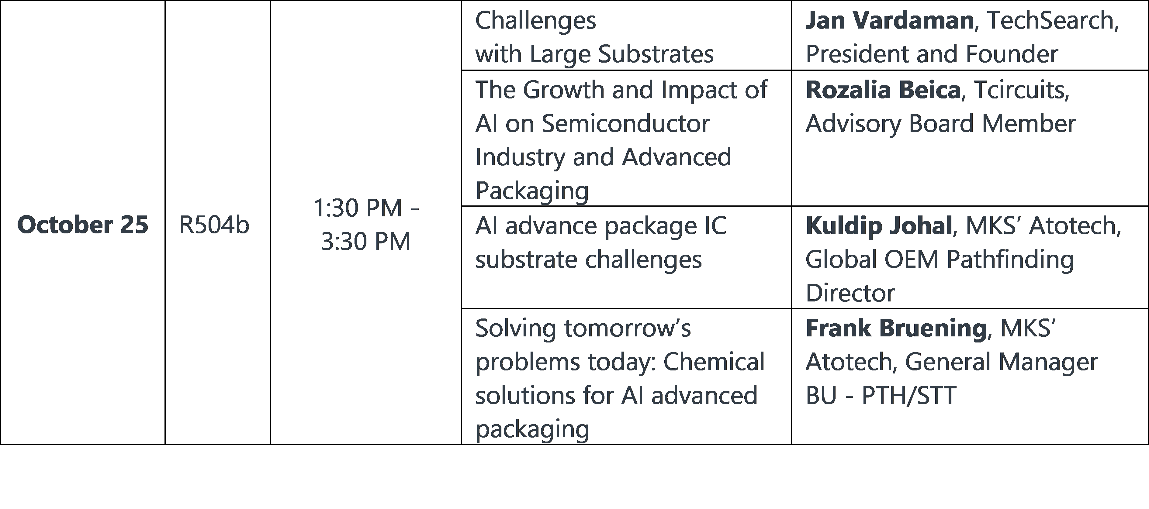
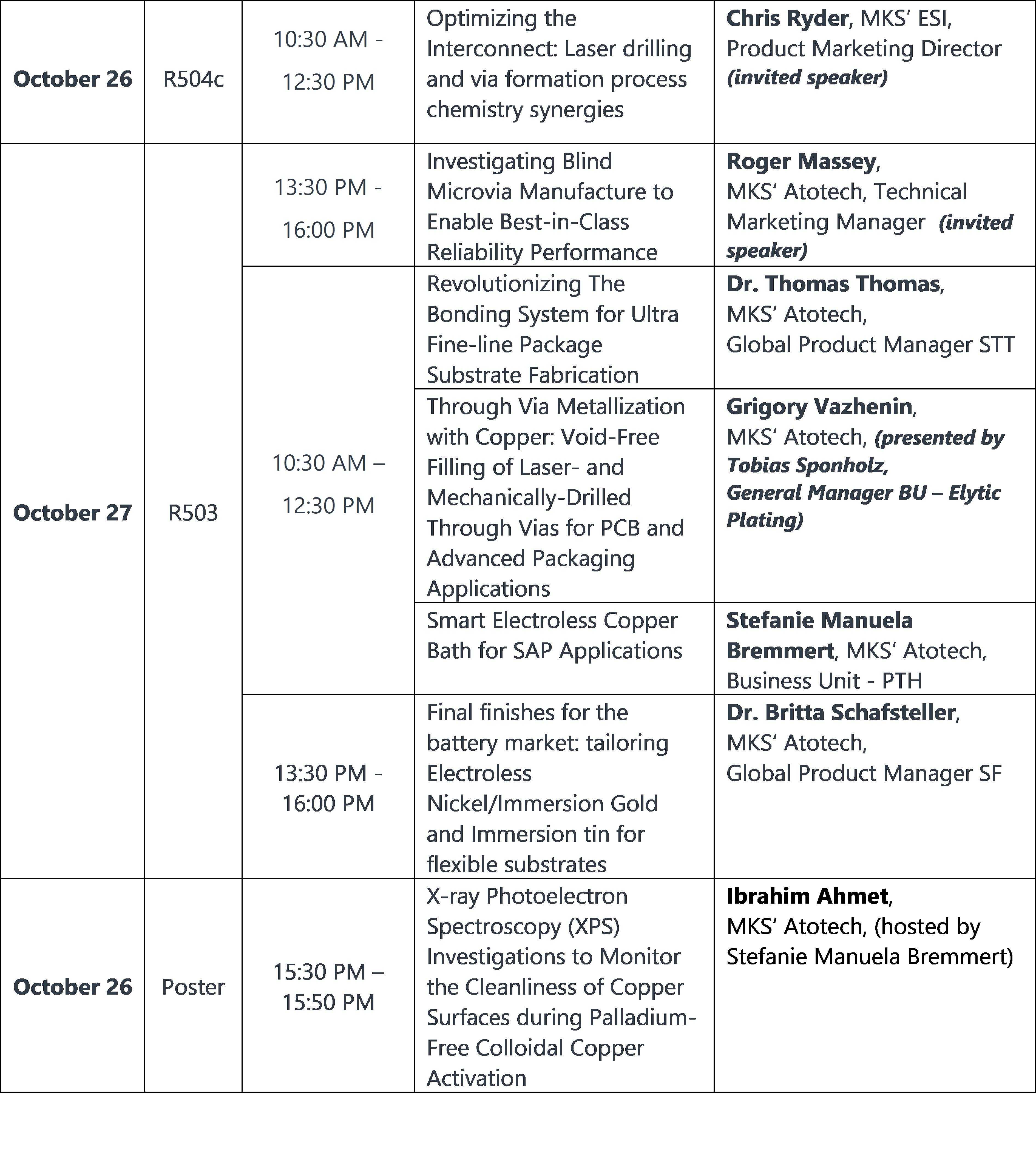
In addition to participating in the exhibition, the team is honored to once again be given the opportunity to host an IMPACT industrial forum. This year the focus is on “AI-enabling innovation in the era of advanced packaging.” The exclusively invited speakers, together with MKS’ Atotech experts, will present four relevant topics/papers on this theme on the 4th floor in room R504b, from 1:30 to 3:30pm on October 25. The team will also present seven additional papers during the general IMPACT technical conference from October 26 to 27, see tables below.
TPCA Show highlights 2023 briefly:
EcoFlash® S300: Differential etching solution suitable for ultra-fine lines on IC substrates.
Novabond® EX-S2: Adhesion promoter suitable for ultra-fine lines and high-speed applications.
CapstoneTM: High-performance/throughput breakthrough productivity for flex PCB UV drilling.
GeodeTM A: CO2 laser system for high precision and high-speed ABF build-up laminate processing.
Cuprapulse® IN: Insoluble reverse pulse plating for high throughput HDI and MLB PCBs.
Cupraganth® MV: New Cu based activator system enabling high yield IC substrates.
Printoganth® MV TP2: State of the art electroless copper process for fine line SAP applications.
Printoganth® MV TP3: Upcoming electroless copper process for super fine lines L/S like 2/2 µm.
Printoganth® P2: Most capable horizontal electroless Cu process for excellent throw into BMVs and nano-void free deposits suitable for advanced dielectric materials (5G, FPCB, etc.).
G-Plate®: New equipment technology for PTH processes of next generation IC substrates enabling highest yields and cutting-edge fine line capability targeting L/S <5/5 µm.
Aurotech® G-Bond 3: New versatile gold bath for nickel/gold, nickel/palladium/gold and palladium/gold plating with non-toxic stabilizer replenishment to prevent the handling of KCN with low gold content and long lifetime.
Stannatech® Flex: tailored immersion tin process for battery flexible board with mitigated substrate and coverlay attack.
PD-Core®: Versatile Palladium plating solution for plating on copper and nickel with low Pd-content and long lifetime for reduced process cost.
Stanna-CAT®: Autocatalytic process for thick tin plating of µ-LED, ICS, or solder depot plating.
Silvertech® C: New silver-plating process that co-deposits 1-2% w/w carbon and produces a highly electrically conductive surface.
Protectostan® LF-E: New sustainable post-treatment to protect the plated tin and tin alloy surfaces of connectors and integrated circuits (ICs) from discoloration under high temperature / reflow and tarnishing under high heat high humidity conditions.
vPlate®: Vertical continuous plating equipment for advanced HDI and IC substrate achieving uniformities of below 7%.
IMPACT MKS’ Atotech Industrial Forum speakers, location and time:
1:30 PM – 3:30 PM | Theme: AI Creating a New ERA of Advanced packaging

IMPACT MKS’ Atotech and ESI Technical Forum speakers, locations and times:

