Atotech’s revolutionary new tool called MultiPlate® for FOPLP
Berlin, 28 February, 2018: At the upcoming IMAPS Device Packaging Conference 2018 next week, Atotech will speak about the move from Fan Out Wafer Level Packaging (FOWLP) to Fan Out Panel Level Packaging (FOPLP).
On Tuesday, March 6, from 11:30 am to 12 pm, Moody Dreiza, Business Director Electronics and Semiconductor for Atotech USA, LLC in North America will talk at the IMAPS 2018 technical conference for Fan-Out, Wafer Level Packaging and Flip Chip about what it means for manufacturing and especially equipment and chemistry to move from round shaped wafers to square shaped panels.
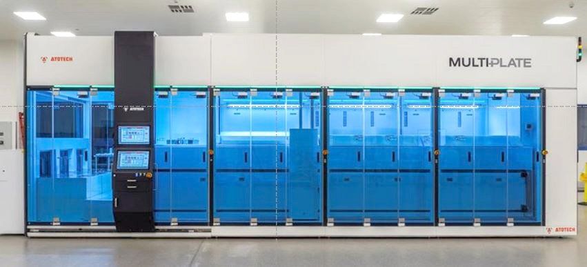
In his presentation, Moody, will specifically discuss what Atotech’s new plating tool “MultiPlate®” can do for FOPLP type of applications. MultiPlate® is Atotech’s new and versatile production tool for wafer-level packaging and panel-level packaging, depending on customer needs. The tool offers the flexibility manufacturers are looking for, while at the same time provides optimal performance in advanced packaging technologies. In combination with Atotech’s newly developed electrolytes for high-speed copper RDL plating for various panel formats, the plated copper deposits show excellent physical properties when plated at high current densities. The tool thereby allows for the deposition of highly pure copper, leading to higher throughput, lower voiding and better reliability.
To learn more about Atotech’s MultiPlate® visitors to the IMAPS DPC 2018 are invited to attend Moody Dreiza’s talk at the technical conference on March 6, from 11:30 am to 12 pm.
Alternatively, visitors can get in touch with several other Atotech product specialists who will be on-site. The IMAPS DPC will be held from March 6 to 8, 2018, at the WekoPa Resorts and Casino in Fountain Hills, USA.