
MultiPlate® and Spherolyte® Cu MD2
The power solution
Fast and reliable
For pure Cu deposits
Simultaneous front and backside plating
Individual side control
For power ICs
IGBTs and power MOSFETs

Designed for the specific needs of modern power ICs. Tool and chemistry deliver a unique solution for IGBTs and power MOSFETs – simultaneous double side plating to effectively reduce and control deposit stress and warpage.
Simultaneous double side Cu plating
- IGBTs and power MOSFETs
- Other wafer types with the need for backside plating
Simultaneous front and backside plating
- Individual control of front and backside plating
- Different Cu thicknesses for both sides possible
- Thick Cu layers of more than 20 µm possible at 5 ASD
Production benefits
- Shortened process flow compared to sequential plating
- Taiko wafer plating
Reliability
- Low stressed Cu deposit 10 mPa after plating
- Zero warpage while plating on both sides
- Uniformity <5% min/max
- Low impurity level
What inspires us
Why we developed MultiPlate® and Spherolyte® Cu MD2
Your challenge
Modern power ICs need metal layers on both wafer sides, front and backside. This requires a strict warpage control during wafer processing.
Our solution
Spherolyte® Cu MD2 and MuliPlate® – Tool and chemistry, the perfect match to plate Cu simultaneously on front and backside of your wafer
Movies
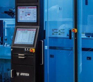
MultiPlate®
An innovative electrochemical plating system for next generation packaging technologies
Contact Us