


Robin Taylor
Marketing and Technical Sales Manager – Electronics
Dear Reader,
The HDI market is continuously evolving to fit new market needs.
The primary growth drivers for change are due to technology shifts towards smaller form factors and designs. This drives industry to increase the interconnection density of the HDI board by reducing line and space dimensions, shrinking via and pad sizes to improve the connection to the next system level and allow for a reduction as required in BGA pitch.
The increasing use of FOWLP in mobile devices, for example, combining an applications processor and memory in a single package with direct chip attach to the HDI board eliminates the need for an IC Substrate. This facilitates thinner packages and smaller HDI boards to allow more room in the mobile devices for the battery.
Atotech is at the forefront of new technology development in the HDI market, to ensure our customers can meet the demanding OEM requirements, with a number of new processes developed specifically for the advanced HDI market.
In this special HDI edition of our Conductor Newsletter we focus on a few key areas for HDI in the articles below.
- BondFilm® LDD mSAP
– Atotech’s Laser Direct Drilling Process for Advanced mSAP - Electrolytic Copper Plating Solutions, Inpulse® and InPro®
– For HDI applications and Fan Out Panel Level Packaging (FOPLP) - Printoganth® T1 and Printoganth® TV
– High throwing power electroless copper solutions - Aurotech® HP
– Market Leading ENIG process for mobile devices - Uniplate® PLB, PLB Cu and Horizon BondFilm®
– Equipment Packages for Electroless and Electrolytic Plating
– Laser Drilling Pre-treatment
We hope you will find this edition of our Conductor Newsletter informative and indicative of our commitment research for our high end customer base.
With best regards
Robin Taylor
Marketing and Technical Sales Manager – Electronics
Publisher: Daniel Schmidt, Head of Electronics Marketing Worldwide
Editor: Yvonne Fütterer, Marketing Specialist Electronics
Product highlights
The changing shape of the HDI market
A move towards smaller and thinner lines and spaces
Figure 1: TSMC’s InFo Package Apple A10 Processor
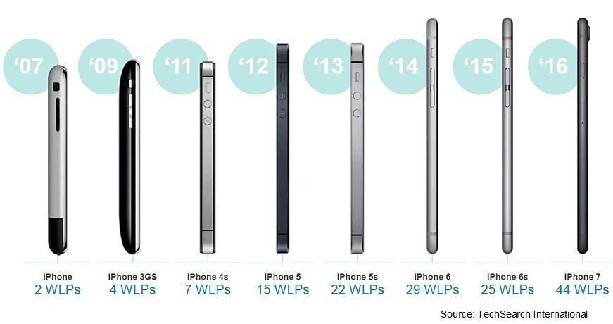
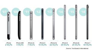
Figure 2: iPhone Thickness and WLP Development by Generation
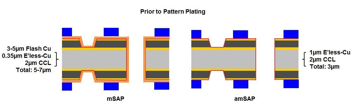
Figure 3: mSAP and amSAP Process Sequences
Figure 5: Impact of Copper Thickness on Line and Space Capability
Figure 6: BGA Design Example
The long term growth forecasts for the printed circuit board market are in the order of 2% CAAGR until 2021 according to Prismark. This varies dramatically by region, so growth is fairly flat. High Density Interconnect (HDI) Microvia, IC Package Substrates and Flexible Printed Circuits (FPC) revenues all declined in 2016 as new designs are smaller and therefore less expensive.
The primary growth drivers for change are due to technology shifts towards smaller form factors and designs. This is not conducive to value or area growth.
Current situation
HDI boards in mobile devices particularly in mobile phones are running out of space and must shrink to accommodate the need for increased space for batteries in our increasingly connected world. This has a number of effects on the HDI market in terms of requirements:
- Increased interconnection density by miniaturization of holes, pads and conductors is required to improve connection to the next system level
– IC Substrate or direct chip attach - This maximizes electrical performance, reducing latency, increasing signal speeds
– Essential for mobile devices, Ultrabook’s and notebooks - Smaller solder spheres and pads require a reduction in BGA pitch which along with thinner PCB’s and die’s raise concerns over warpage and solder joint reliability
In conjunction with all of these requirements improved shielding is needed with more components crammed into a smaller space. Shielding may also be incorporated into the HDI PCB going forward and improved thermal performance of the HDI PCB is driven by mobile devices to reduce heat dissipation.
This is quite a list of requirements for the HDI market. We have already seen the introduction of High Density Fan Out Wafer Level Packaging (FOWLP) in mobile devices with the advent of TSMC’s Integrated Fan Out (InFo) package combining an Applications Processor (AP) and Memory in a Package on Package (PoP) build on the Apple A10 processor in the iPhone 7 (Figure 1).
This eliminates the need for an IC Substrate and has impressive performance metrics, higher system-level performance in a thinner package, at a cost.
Where is the market going?
Whether other mobile phone suppliers will follow suit remains to be seen, albeit it has been reported that Samsung will introduce this in its next generation devices. We can assume for high end mobile devices that this will result in a huge increase in direct chip attach to HDI boards in the future.
Direct chip attach for InFo and others will result in a very low warpage requirement and an underfill requirement under the AP/Memory stack.
The tendency towards smaller, thinner PCB’s and die’s to improve mobile device form factor is clearly shown in the development of the iPhone thickness below. The advances in HDI development and increasing levels of Wafer Level Packaging (WLP) in the devices enable this. The number of WLP’s has also significantly increased the reliability of mobile devices (Figure 2).
New laser drilling developments are required to ensure that smaller vias can be mass produced at reasonable cost and also to reduce the Heat Affection Zone (HAZ) in the dielectrics which limits via density.
New lasers with picosecond and femtosecond pulses are coming to market offering increased speed and productivity with improved quality and less HAZ at lower hole sizes. This is a critical development to enable ultra small microvias <25µm in prepreg going forward. Improved surface treatments for copper to extend the life of CO2 Laser Direct Drilling (LDD) are also coming to the market.
Next generation designs for HDI will see a reduction to ≤ 30 µm line and space (L/S). This excludes substractive patterning techniques which have been the mainstay used in HDI production up until now. The PCB industry is already moving towards mSAP and amSAP technology to achieve latest requirements. Thinner copper foils are required and design rules also have to change to meet these new demands (Figure 3).
The reduction in copper foil thickness increases customer capability to produce fine L/S as the copper thickness on the dielectric is critical to both yield and L/S capability (Figure 5). Ultra low profile copper foils are also required which increase cost.
Design for manufacture is also very important (Figure 6).
The “headline” L/S number, in the example above 30µm, is very often much lower than the average L/S, to ensure yields are high. In this example it is around 45µm L/S, typical for the iPhone 7 for instance.
“Ultra HDI” designs are approaching SAP dimensions, for example a BGA pitch of 225µm with double trace routing requires 20µm L/S with a pad diameter of 125µm. This is already targeted for manufacture in 2017-2018 in Asia.
Challenges and Solutions
Every aspect of HDI PCB manufacture is challenged to meet these market needs:
- Surface preparation and multilayer bonding
– LDD preparation, dry film adhesion and copper to dielectric bonding - Desmear
– Small via desmear - Electroless copper
– High throw electroless copper for small microvias - Electrolytic copper
– Electrolytes capable of via filling and pattern plating simultaneously
– Through hole filling electrolytes - Final finishes
– Must evolve to meet finer L/S requirements and smaller pad diameters to ensure solder joint reliability and electrical performance
For many of the challenges, Atotech has developed innovative solutions of which some are discussed in this edition of the Conductor.
For more information, please contact:
Robin Taylor
Marketing and Technical Sales Manager Electronics at Atotech Deutschland GmbH
Phone: +49 (0)30 – 349 85 1615
Email: robin.taylor@atotech.com
Product highlights
BondFilm® LDD MSAP – Atotech’s Laser Direct Drilling pretreatment for advanced mSAP applications
The latest additions to the highly successful BondFilm® family
Figure 1: Process flow for BondFilm® LDD MSAP + LDD MSAP Enhancer

Figure 2: Via size versus Cu content
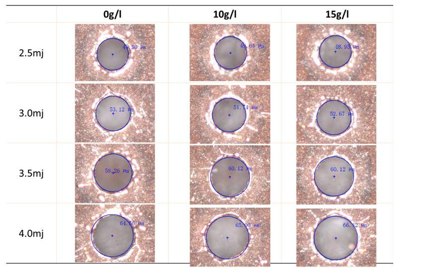
Figure 3: Detailed via opening results employing BondFilm® LDD MSAP at 0.5 µm as pretreatment across the copper leading curve
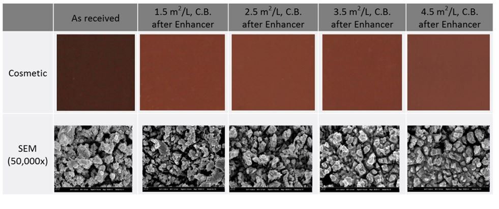
Figure 4: Non etching organic removal by BondFilm® LDD MSAP Enhancer – solution can be used up to 4.5 m²/L cut board
Since its first introduction in 1999, Atotech’s BondFilm® product family has been and remains to be the world’s most successful, reliable and omnipresent oxide replacement process for inner layer bonding and LDD pretreatment. Our continuous work on the product range of the BondFilm® family in light of ever changing market needs and developments has led to the most recent additions to this product family – BondFilm® LDD MSAP and BondFilm® LDD MSAP Enhancer.
Changing market needs
BondFilm® solutions for LDD pretreatment have been on the market for several years now. They are characterized by high reliability, easy handling and high throughputs. These are all clear advantages versus Black Oxide processes which is why so many customers have opted to use BondFilm® products for LDD pretreatment. Standard applications in the HDI space normally require an etch depth of 2-3 µm in order to prepare the surface for best laser absorption. With the changing demand on HDI manufacturing processes, however, the demand for chemical processes employed has changed.
Customers have started to move towards the application of mSAP manufacturing where the copper base before the LDD process can be as thin as 3-5 µm. This also led to the need to further reduce the etch depth of 2-3 µm while improving the via creation performance and stability. At the same time, the need grew for a non-etching post-dip that removes all organic residues from the surface and optimally prepares the board for the subsequent PTH process.
BondFilm® LDD MSAP and BondFilm® LDD MSAP Enhancer
With the development of BondFilm® LDD MSAP and BondFilm® LDD MSAP Enhancer, Atotech meets these new requirements. The process follows the standard BondFilm® process flow (see figure 1) and is suitable for use with BondFilm® Horizon process equipment, offering a complete system solution. It offers uniform roughness and surface characteristics for an improved efficiency of laser absorption already at a target etch depth of 0.5 µm. As minimization of copper removal is the target of this process, a non-etching post-treatment was also introduced.
Tests and results
Extensive testing of the process was done in our TechCenter in Guangzhou, China in collaboration with an external partner for Laser Direct Drilling. After LDD pretreatment with BondFilm® LDD MSAP a range of laser energies was tested. The optimal via size (target 50 – 65 µm) was achieved at very low laser energies, between 3-4 mj. (figure 2 and 3).
Additionally and as requested by customers, BondFilm® LDD MSAP Enhancer is a non-etching post-dip which removes the organic layer from surface below detection limits before the Plating Through Hole (PTH) process, without etching the surface at all (figure 4).
Achievements
By being perceptive, foreseeing trends and carefully listening to customer needs, our team of experts and specialists was able to react to the ever changing market needs and develop this innovative, yet simple, low-temperature pretreatment process – BondFilm® LDD MSAP. It perfectly prepares the surface for laser direct drilling at a very low etch depth of only 0.5 µm and is suited for conveyorized applications for thin material handling such as copper foils used for mSAP build ups.
Together with the post-treatment BondFilm® LDD MSAP Enhancer, which prepares the surface for subsequent process steps (PTH), it is the perfect combination to optimize the operation of mass production CO2 lasers in an environment for mSAP applications.
For more information, please contact:
Stephan Hotz
Global Product Manager Surface Treatment Technologies at Atotech Deutschland GmbH
Phone: +49 (0)30 34985- 534
eMail: Stephan.hotz@atotech.com
Product highlights
Electroplating solutions for next generation products
Atotech’s innovative pattern plating portfolio for advanced HDI utilizing mSAP/ amSAP and panel level packaging
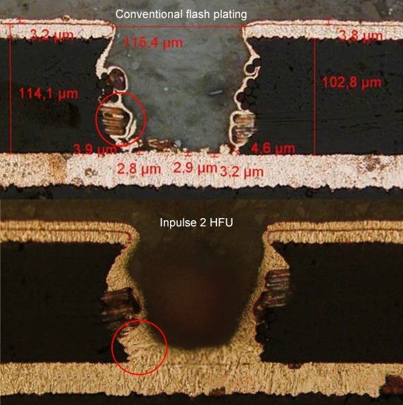
Figure 1: Inpulse® 2HFU – Excellent BMV levelling
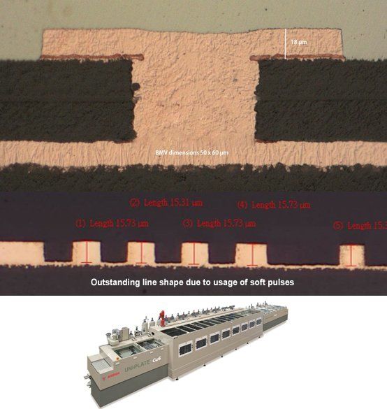
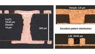
Figure 2: Inpulse® 2MSAP – good filling performance for BMV
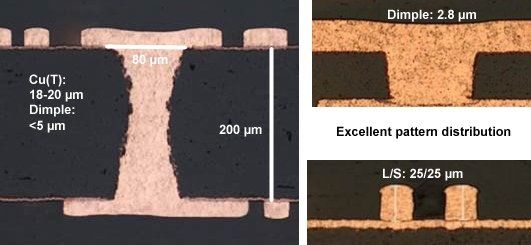
Figure 3: InPro® THF – excellent filling for TH and BMV
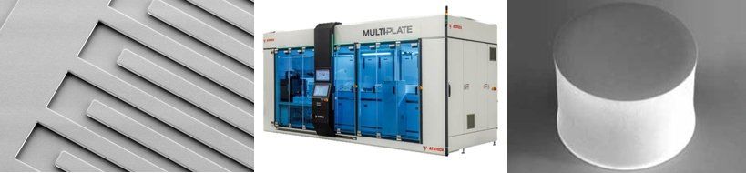
Figure 4: MultiPlate® with Innolyte® PLP and Innolyte® P – RDL and Cu plating for Fan-Out packaging
Latest smartphone and tablet generations will have higher functionality and data transfer speeds. This can only be achieved with more complex HDI designs and a higher density of features. As a result, line/ space requirements are getting tougher and HDI manufacturing technology is being transferred from panel plating to pattern plating.
In amSAP the pattern plating is made directly on e’less copper whereas in mSAP flash plating is applied after deposition of e’less copper. The flash plating step allows stronger etching after the dry film (DF) process which ensures best capture pad cleanliness. Atotech offers a portfolio of solutions and innovative products to achieve the new requirements and best (a)mSAP pattern plating results.
Inpulse® 2HFU and Uniplate® P/LB/Cu
A drawback of high-speed laser drilling (higher energies – less number of shots) is the formation of hole-wall roughness and gaps. Standard copper reinforcement processes cannot cover some of these drilling defects entirely. Atotech’s Inpulse® 2HFU process for flash plating in Uniplate®, however, can solve this problem and leads to best BMV preparation for the subsequent copper filling. This special Inpulse® 2HFU electrolyte gives excellent throw to the BMV and overcomes hole wall roughness as well as BMV “wedge voids”. Using it together with Atotech’s Uniplate® P/LB/Cu system allows inline wet-to-wet strike plating directly after e’less metallization.
Inpulse® 2MSAP together with Uniplate® IP2
For the pattern plating step, Atotech’s latest electrolytic plating system Uniplate® IP2 Pattern is now available. Together with the new Inpulse® 2MSAP process for horizontal pattern BMV filling it allows safe transportation and reliable filling of pattern structures of lines/spaces (L/S) of 30/30 µm. The high applicable current densities and the applied pulse plating lead to a short processing time of less than 30 min for 20 µm Cu plated together with excellent line shape for best signal processing.
InPro® THF for (a)mSAP applications
Chemicals used for Vertical Conveyorised Plating lines (VCP) also need to be compatible to the corresponding equipment in order to achieve optimum production results. For VCP equipment, Atotech has developed the new InPro® series. It is designed for use with insoluble anodes and direct current (DC) rectification. Within the InPro® product portfolio we offer solutions for conformal plating, pillar plating and filling of blind micro vias (BMV) and through holes.
The new InPro® THF process provides reliable BMV filling performance at high current densities up to 3 A/dm² especially for (a)mSAP application in mass production. The process shows no tendencies for necking or dome plating for best subsequent process compatibility. It may also be used for TH filling applications for advanced package substrate technology. The filling with copper instead of plugging material offers advantages when it comes to reliability (thermal stress) because of different CTE’s. In order to meet the technological and yield requirements for next generation HDI and packaging, the process provides pattern plating with excellent pattern distribution.
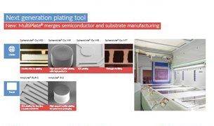
Innolyte® with MultiPlate® for panel level packaging
Atotech developed the MultiPlate® system to meet the demand of increased interconnection density by miniaturization of holes, pads and conductors and the introduction of High Density Fan-Out Wafer Level Packaging (FOWLP). MultiPlate® was designed to provide a full system solution, including equipment and chemical processes, for wafer application and is now also available for panel level applications (FOPLP).
Fan-Out Wafer Level Packaging was introduced some years ago and is now seen as a key advanced packaging platform to meet the technological and cost requirements of the industry. To produce substrates at high yield and low costs substrate manufacturer try to utilize their infrastructure and cost advantages. This currently drives the industry and the supply chain – the transfer of FOWLP to FOPLP.
Atotech’s new Innolyte® series is designed to be used in the MultiPlate® Panel for high speed Cu deposition in RDL layer plating with and without micro vias as well as tall pillar plating (PoP design). The combination of new electrolytes that enable high speed Cu deposition with an adapted plating equipment technology will be the answer of the challenges the advanced packaging industry currently faces.
For more information, please contact:
Henning Huebner
Global Product Manager Panel / Pattern Plating at Atotech Deutschland GmbH
Phone: +49 30 – 349 85 434
Email: henning.huebner@atotech.com
Product highlights
Printoganth® T1 and Printoganth® TV- High throw electroless copper processes
Atotech’s metallization answers to the increasing miniaturization requirements for advanced HDI utilizing mSAP and amSAP technology
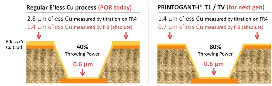
Figure 1: E’less copper deposition thickness comparison
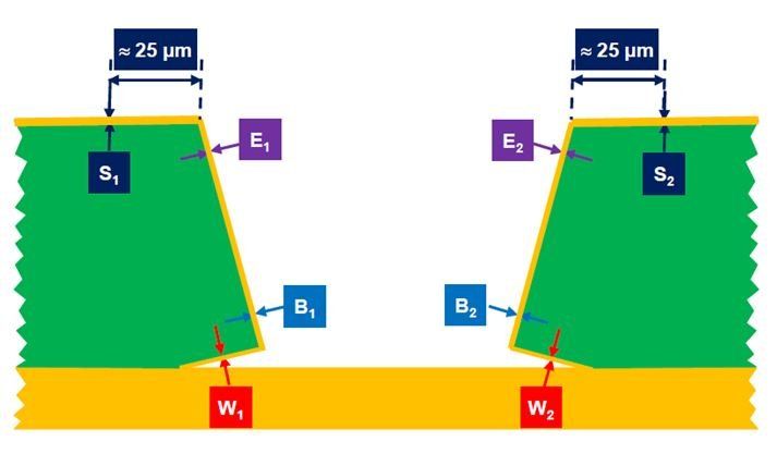
Figure 2: TBD
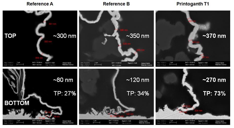
Figure 3: Throwing power comparison of Printoganth® T1 and two reference processes
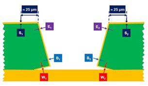
Background
Next generation designs for HDI will see a reduction to ≤30µm lines and spaces (L/S). This excludes semi panel plating techniques which have been the mainstay used in HDI production up until now. The PCB industry is already moving to Modified Semi Additive Processing (mSAP) and Advanced Modified Semi Additive Processing (amSAP) to achieve this capability and to improve yields. These advanced manufacturing technologies require a thicker electroless copper deposition in the BMVs compared to the panel plating process, primarily due to reliability concerns. In order to ensure highest reliability and excellent copper-to-copper interconnection on the capture pad, typically copper etching prior to the via-filling process steps is applied to remove copper oxide and potential dry film residues. In contrast to the semi panel plating techniques, for amSAP technology the total copper thickness at the side walls of the BMVs is only build-up by the electroless copper process and not by an additional strike e’lytic copper process prior to via filling. As a consequence, the copper thickness at the BMV side walls is very thin, thus extensive copper etching to clean the capture pad is not viable because of the attached risk of voiding.
In order to allow for soft etching – and a clean copper to copper interconnection – manufacturers explore the possibility to increase the absolute e’less copper thickness at the bottom of the BMV to over 0.5 µm. As a matter of fact, the electroless copper thickness at the surface of the build-up layer is increased as well.
Key advantage
The new high throwing power electroless copper processes Printoganth® T1 for application in horizontal plating equipment and Printoganth® TV for vertical panel transportation offer the major advantage of reducing the absolute electroless copper thickness on the surface to a minimum while achieving the copper thickness targets in the BMV. Compared to established e’less copper processes for panel plating, the fine line resolution and process costs are significantly improved because the absolute copper thickness that needs to be (differentially) etched for the pattern formation is reduced – as illustrated in figure 1.
Throwing power performance
The throwing power performance of the new processes is shown exemplarily for the horizontal process Printoganth® T1 that was compared with two mass production proven horizontal reference systems (see figure 2). The test was carried out in Uniplate® LB horizontal mass production equipment, which is the standard production environment for high-end HDI manufacturing. Reasons for this are the constant process conditions for each panel and excellent fluid exchange especially in BMVs. During the test, the electroless copper thickness at the entrance of the BMVs was comparable for all three processes fluctuating around 350 nm. However, the absolute thickness at the bottom of the BMVs was significantly higher for Printoganth® T1 compared to the reference systems. This TP result of about 70 to 80% was reproduced several times in different line tests using a variety of base materials.
Summary
Printoganth® T1 and Printoganth® TV are Atotech’s electroless copper answers to increasing miniaturization requirements of the high-end HDI market segment. Both processes enable high throughput and reduced electroless copper surface thickness in order to reach the target copper thickness in the BMVs in reasonable plating times compared to established electroless copper processes.
For more information, please contact:
Tobias Sponholz
Assistant Product Manager Plating Through Hole at Atotech Deutschland GmbH
Phone: +49 (0)30 – 349 85 1573
Email: tobias.sponholz@atotech.com
Product highlights
Aurotech® HP – Market leading product for mobile device OEMs
ENIG for next generation HDI

Figure 1: Aurotech® HP – Process description
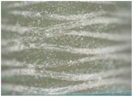
Figure 2: Metal residue free base material
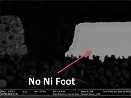
Figure 3: The prevention of nickel foot to maximize resolution
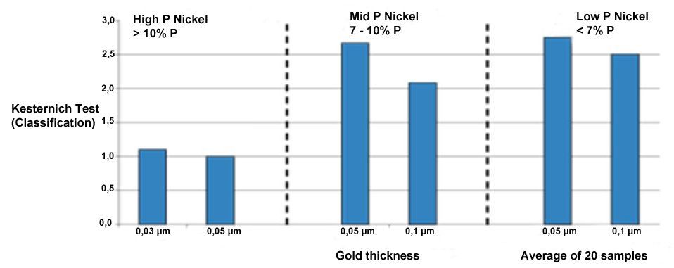
Figure 4: Environmental corrosion performance demonstrated by the Kesternich test
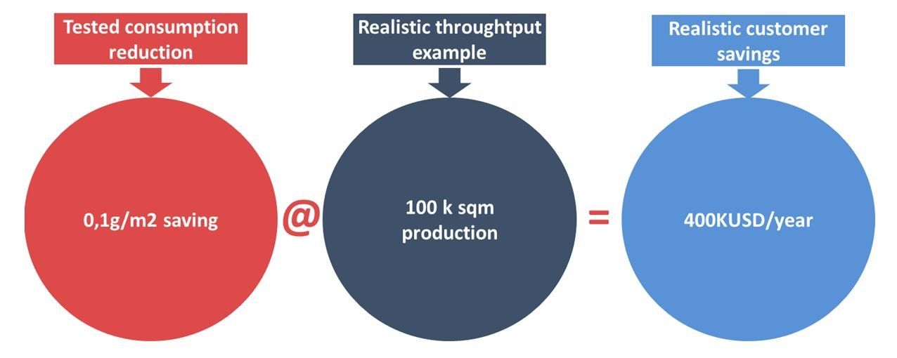
Figure 5: Impact of optimized distribution on cost with Aurotech AU Plus
Figure 6: Controllable parameters
The next generation HDI is equally synonymous with mobile devices as traditional HDI. The next generation, however, not only has to accommodate further decreasing form factors but also has to cater for sulphur rich environments. The final statement theorizes that the dominant market will be China.
Atotech’s Aurotech® HP ENIG process conforms to and satisfies the requirement of the market leading mobile device OEMs. In this capacity the process is enjoying production proven success.
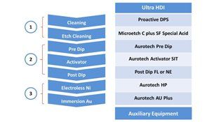
In Aurotech® HP, we offer a customer proven system, based on a systematically optimized process, which can uniquely cater for the nuances of the next generation HDI circuitry:
- Pretreatment (cleaner and microetch)
- Activation (predip, activator and post dip)
- High quality plating (electroless nickel and immersion gold)
1. Pretreatment: The removal of inherited artefacts and conditioning of the copper surface
Proactive DPS is designed to remove any inherited residual metals from the base material after circuitization. The source of these metals can be the copper to base material adhesion promoters and/or remnants of the metallisation (PTH) activation step. This is especially true of colloidal activation system. Failure to deal with these issues may result in shorts in a fine line production environment.
Proactive DPS in combination with DPS Microetch C with SF Special Acid, ensures the foundation for confident fine feature production.
2. Activation: Optimized initiation coupled with high resolution
For those in the know, the avoidance of nickel skip and high resolution circuitry without spreading are contradictory requirements. Never the less, the Aurotech® HP activation system combining Activator SIT and Post dip FL or NE, has made it possible to activate adequately to cope with low loading factor second image technology type (SIT) production whilst also preventing any potential nickel spreading due to the precipitation of hydrolyzed palladium in hard to rinse locations.
3. High quality plating: Effective diffusion and corrosion prevention with cost benefits
The 4 MTO capable electroless nickel, Aurotech® HP, is the flagship for this process. The high phosphorous nickel (>10% P), as previously hinted upon, is a requirement from the leading mobile device OEMs. The amorphous nickel structure guarantees market leading environmental and chemical corrosion performance.
In addition to excellent environmental corrosion properties, the potential for nickel corrosion from the gold becomes negligible.
Aurotech® AU Plus is a reduction assisted immersion gold process which by virtue of mechanism virtually eliminates nickel corrosion even on mid phosphorous nickel systems. Whilst the low nickel corrosion is a significant attribute, the cost saving potential is truly interesting to customers. To achieve true savings, the key is good gold distribution. A better distribution between the pads and the PTHs makes it possible for the minimum gold thickness to be targeted rather than a thicker, compensatory thickness to ensure gold thickness compliance. In production simulations a saving of 0,1 g/m² in gold salts could be achieved. The implications of such a saving are simulated in Figure 5.
Auxiliary equipment is also available to further enhance process control and saving. The parameters displayed in Figure 6 can be controlled.
For more information, please contact:
Rick Nichols
Global Product Manager Selective Finishes at Atotech Deutschland GmbH
Phone: +49 (0)30 – 349 85 340
Email: rick.nichols@atotech.com
Product highlights
Atotech’s equipment solutions for mSAP and amSAP
Innovative integrated horizontal system solutions for next generation HDI manufacturing
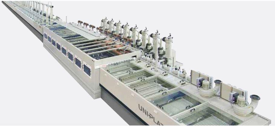
Figure 1: Uniplate® PLBCu6
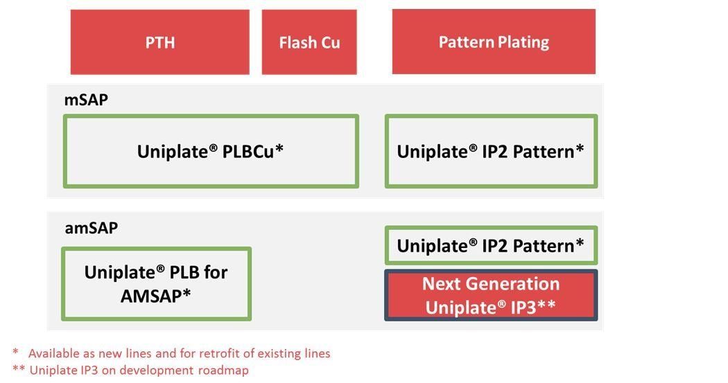
Figure 2: Uniplate® for mSAP and amSAP overview
Figure 3: Uniplate® PLBCu6 inline wet-to-wet process)
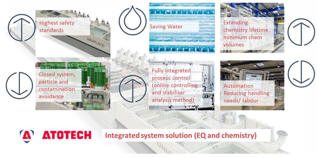
Figure 4: Solutions available for mSAP and amSAP

Figure 5: Horizon BondFilm® equipment highlights
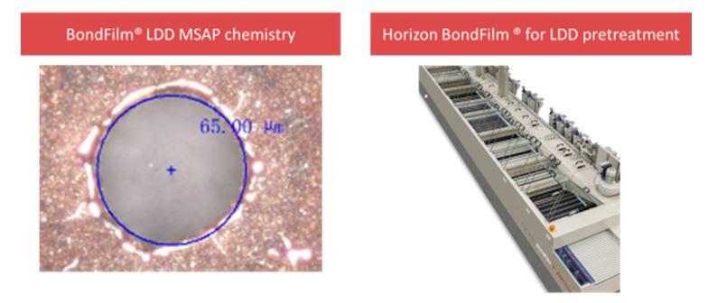
Figure 6: BondFilm® LDD MSAP and Horizon BondFilm®
Next generation designs for HDI will see a reduction to ≤ 30 µm line and space (L/S). This excludes substractive patterning techniques which have been the mainstay used in HDI production up until now. The PCB industry is already moving towards mSAP and amSAP technology to achieve latest requirements. Thinner copper foils are required and design rules also have to change to meet these new demands.
Uniplate® PLBCu6
Today Atotech is the only company that can provide a complete inline process solution from desmear, electroless copper to electrolytic flash copper plating. One key benefit of the inline process is that after the electroless copper process step no handling of the PCB is necessary, which decreases any operational need, as well as further reduces the risk of contaminations to the PCB in between the electroless copper and the electrolytic flash copper plating steps.
Atotech’s Uniplate® PLBCu6 incorporates innovations that allow significant savings of water and energy while at the same time extending the life time of the chemistry used. The system utilizes the Securiganth® E series for desmear, Printoganth® U Plus or Printoganth® T1 for PTH and Inpulse® 2HFU for electrolytic copper plating to achieve superior throwing power and uniformity.
For finer line and space requirements our Uniplate® provides several universal transport system solutions to accommodate thin copper clad. For example, UTS – xs transportation system allows the safe transport of materials down to 40 μm core + 2×2 μm copper clad. In addition, we are able to offer solutions for the avoidance of particles and a sophisticated filtration package for fine line structures.
With this and many more features Atotech’s Uniplate® PLBCu6 is designed to produce outstanding reliable interconnects at a very high throughput while minimizing handling needs and consumption of resources.
System features and benefits:
- Entirely inline process with no handling needs and optimized footprint
- Significantly reduced water and energy consumption
- Seeking to optimize and extend the lifetime of chemistry
- Process fully controlled via VCS
- Real time copper control in electroless copper bath for leading process stability
- Automatic cleaning cycles reducing operator capacities
- Sophisticated particle reduction and filtration packages available
- Highly reliable metallization of through-holes and BMVs
- Excellent throwing power and uniformity
- Inert and segmented anodes avoiding oxygen and sludge formation
Uniplate® PLB for amSAP
Over the past years, the design of high-end printed circuit boards has become increasingly challenging for manufacturers. In particular finer lines and spaces below 30/30 μm require new technologies such as the advanced modified semi-additive process (amSAP). This reduces the differential etch depth during the pattern formation. Furthermore, thinner materials need to be processed in a reliable manner. In addition, particle control is highly important for the yield of the manufacturing process.
Atotech’s integrated solution consisting of the mass production Uniplate® PLB equipment and the reliable Printoganth® U Plus or Printoganth® T1 electroless copper process enables manufacturers to master the challenges ahead, e.g. thin material processing, particle control, dry film adhesion, thick electroless copper and optimization of operating cost.
Uniplate® PLB for amSAP features and benefits:
- Inline process from desmear until after electroless copper (no handling in between process steps, wet to wet and high throughput)
- VCS controlled for superior process control
- Totally encapsulated (retaining fumes, heat, evaporation)
- Efficient rinsing technology (3x & 4x rinses saving water and waste)
- Superior Throwing Power in BMVs and THs and surface distribution
The benefits of the Uniplate® system are multifold and include superior panel to panel uniformity and traceability, significant savings in chemistry, high efficiency fluid management and delivery, and an automated cleaning system and cycles which saves manpower and yield.
Horizontal Pattern Plating with Uniplate® Cu IP2 Pattern
and next generation Uniplate® Cu IP3
Uniplate® Cu IP2 Pattern
Atotech’s Uniplate® Cu system (InPulse® 2) is now also available for pattern plating. The line is installed at our Yokohama TechCenter and we are processing samples for our customers. Our current system capability for mSAP is: 150 µm to 1,200 µm panel thickness; with 30/30 µm line and space. The new adjustments to our standard Uniplate® IP2 for pattern plating ensure safe and damage free thin copper transportation and result in an optimized copper distribution:
- New roller design (ADF and super slim): safe and damage free transportation
- New design foil guides: safe and damage free transportation and best copper distribution on the surface
- Particle reduction and avoidance features made of avoidance of crystallization via spray nozzles, suction system for clamp drive, fine line filtration (1µm -2µm absolute) with high flow filters in Cu modules Double Cu Dissolving Tank with Fe/Cu Analyzer for an online control and stable bath solution parameters
The Uniplate® Cu IP2 Pattern plating line can be delivered as a new line or can be retrofitted into existing UTS-s or UTS-xs Plater with a retrofit package. Customers are kindly invited to process samples at our pilot line in our Yokohama TechCenter.
Next generation Uniplate® Cu IP3
To keep up with technological advancements and to have a solution for upcoming requirements in the development of mSAP and amSAP technology, we started the UniPlate® IP3 project with the main target to improve primarily plating surface distribution and transportation capability of very thin 25 µm + 2*2 µm Cu panels with minimal bending behavior. The development work is conducted at Atotech’s R&D Headquarter in Berlin and in Feucht.
Key system developments:
- New roller design (ADF and super slim): for safe and damage free transportation
- New flex clamps will have a better closing mechanism to avoid panel bending and ensure a reliable clamp contact for an optimum current transmission
- New optimized anode segmentation and new rectifier for a better and more uniform copper distribution
- Advanced spray piping rack for better fluid exchange and safer and damage free panel transportation
The next generation Uniplate® Cu IP3 will be suitable for panel and pattern plating for all types of applications. After the initial testing phase of the new UniPlate® Cu IP3 plating line and successful beta site testing with customers, the expected market release is planned in Q2 2018.
Horizon BondFilm®
Customers moving to mSAP driven by major OEMs also have a requirement for high precision laser direct drilling application on thin copper foils (3-5 µm thick) with via targets of 50 – 65 µm. Finer lines and spaces require thinner copper clad. Thinner copper clad requires a very uniform etch rate and high efficiency at low etch depths.
For this, we have created BondFilm® LDD MSAP to be run in Atotech Horizon BondFilm® equipment. Atotech therewith provides a solution for latest requirements for high precision LDD application on thin copper foils.
The BondFilm® LDD MSAP process and equipment offers a better LDD performance by improving the laser absorption on the surface. The Horizon BondFilm® line ensures superior performance at lowest etch depth and excellent uniformity via process control and traceability.
Horizon BondFilm® features and benefits:
- Safe horizontal transportation system UTS-xs
- Fine Line Filtration with 5 µm cartridge filters
- Conductivity monitoring in the final rinsing step
- Outlet module equipped with contactless electrical discharge unit
For more information, please contact:
Felix Schmidt
Manager Business Development Equipment worldwide at Atotech Deutschland GmbH
+49 (0)9128 725 633
Email: felix.schmidt@atotech.com
Or:
Andreas Schatz
Global Product Manager Electronics Equipment at Atotech Deutschland GmbH
+49 (0)9127 725 615
Email: andreas.schatz@atotech.com
Trade show news
Thoughts and impressions from ECTC 2017
Technology Report
Figure 1: Latest technology developments and solutions for next generation FO-PLP

Figure 2: Atotech’s MultiPlate® equipment and plating processes for next generation FO-WLP and FO-PLP
ECTC’s excellent technical program and the number of key semiconductor industry people in attendance makes it a must attend event. There is a huge amount of content, both technical and market trend focused, as well as a plethora of exhibitors.
Papers are divided circa 50:50 between industry and academia which gives both a good market overview and a look into the future, and to where industry is cooperating with academia. Close to 1550 attendees and nine concurrent streams made this a very busy few days.
As with last year there was a high focus on Fan Out Wafer Level Packaging (FOWLP) with focus also on Panel Level Fan Out (PLFO) in a plenary session, with industry experts from TSMC, Nanium, Fraunhofer, Deca and Qualcomm discussing the whys, and wherefores of PLFO.
The panel was of the opinion that fan-out will eventually transition from wafer level to panel level in the not too distant future,( a vision that was not necessarily agreed to by many in the audience) however there are many hurdles to overcome:
- Solving process issues and materials to allow the use of larger formats
- Whether that be 450mm wafers or panels
- Particularly related to warpage control, die shift after overmolding and registration of RDL layers
- Standards, design constraints, inspection and potential yield issues with panel formats
Doug Yu from TSMC remarked that he sees great potential for PLFO “There is high risk, but it will be here eventually”.
“Panel and wafer are manufacturing formats, not technologies and fan out is a design, not a technology” explained Steffen Kroehnert from Nanium. He also made the comment “We already have 50 Shades of Fan Out, we don’t need any more”.
The differential between High Density Fan Out (HDFO) with multiple layers of fine line RDL and parts currently made in wafer formats but using low density circuitry was highlighted by Steve Bezuk from Qualcomm who noted that many of their low-density designs with 10-15µm line and space are ideally suited to PLFO.
Tim Olson from Deca said PLFO “Could reduce costs by 30% due to capital investment reduction and material efficiency improvements”.
The general opinion is that PLFO will initially focus on cost reduction with low density designs of maybe a single RDL layer whilst looking to evolve to HDFO over time but this will take some time.
Many of the technical presentations focused on fan out and ways to reduce warpage by adjusting the CTE of the glass carriers to better fit to the packages produced.
There was also significant focus on heterogeneous integration particularly at Luncheon Keynote, delivered by Babak Sabi, Corporate Vice President and Director of Assembly and Test Technology Development, Intel Corporation, who reiterated many of the concerns of other key players in the industry on:
- Package scaling and on package heterogeneous integration
- Multi Chip Packaging
- Use of High Density Fan Out for heterogeneous integration
For High Performance Computing (HPC) there is a need for a new barrier layer metal to replace nickel for high current applications and in general as we move towards 5G where the higher frequencies will require a new surface finish. There were some papers from academia / industry on Cobalt, Tungsten, Phosphorous (CoWP) ternary layers which show great promise as a barrier layer and on Electroless Palladium Autocatalytic Gold (EPAG) in this area.
From a surface finish perspective there were also interesting papers on all copper interconnects from chip to substrate or chip to chip.
Overall an excellent technical conference with too many subjects to mention as well as excellent interactive poster sessions.
For more information, please contact:
Robin Taylor
Marketing and Technical Sales Manager Electronics at Atotech Deutschland GmbH
Phone: +49 (0)30 – 349 85 1615
Email: robin.taylor@atotech.com
Trade show news
Global events and trade shows
Past Events
Atotech participated in a number of key global events during the past few months. Here’s a quick highlight:
JPCA Show 2017
As “The total solution exhibition for electronic equipment 2017”, the JPCA Show took place from June 7 to 9, 2017, at Tokyo Big Sight in Tokyo, Japan. Highly specialized and focused with large international attendance, the show’s main theme was “Mount, connect, manufacture, and expand in The Total Solution Exhibition”. The main subjects on the floor were modified Semi-Additive Process (mSAP) and fan-out wafer level packaging (FO-WLP) with many lectures, process materials and manufacturing equipment.
At the show’s Press Forum, NovaBond® IT, Atotech’s new and innovative non-etching adhesion promoter for IC substrates and high frequency application inner-layer bonding and soldermask pretreatment, was presented to press and media. In addition, Atotech experts were ready to discuss a multitude of topics at Atotech’s booth and participated at JPCA’s New Product Introduction (NPI) Forum with two presentations:
- Electrolytic plating solutions for advanced IC substrates and beyond
- Horizontal electroless copper solutions for next generation package substrates
Copyright: IEEE Electronics Components and Technology Conference 2017
ECTC 2017
The Electronic Components and Technology Conference (ECTC) is one of the premier international events, bringing together experts and specialists in packaging, components and microelectronic systems science, technology and education. Held from May 30 to June 2, 2017, at the Walt Disney Swan and Dolphin Resort in Florida, USA, the show provided the perfect place for Atotech to present its next generation plating technologies for FO-Panel Level Packaging (FO-PLP). Ralph Zoberbier, Manager Equipment Sales and Marketing at Atotech Deutschland GmbH, presented current manufacturing challenges in panel based packaging applications and highlighted latest technology developments and solutions on Atotech’s MultiPlate® equipment and plating processes, dedicated for next generation FO-PLP.
Atotech experts also co-authored work which was presented at the ECTC Show 2017:
- “Scaling Cu pillars to 20μm pitch and below: Strategic role of surface finish and barrier layers” presented the first demonstration of Cu pillar interconnections at 20μm pitch, enabled by innovative interconnection designs and advances in surface finish metallurgies with precisely controlled and unique interfacial reactions.
- “Morphology study of bimodal-particle-based all-copper interconnects formed at low sintering temperature” presented the main advantages of dip based, all-copper interconnect technologies.
C-Tex Show 2017
Atotech exhibited and presented at the C’Tex Show 2017, which was held from May 17 to 19, 2017, at the Suzhou International Expo Center in Suzhou, China. Under the Shows topic “Advanced Circuits – Leading the PCB industry to innovation”, Paul Yang, Assistant Business Manager East China at Atotech China Chemical Ltd., presented Atotech’s horizontal solutions for “Next generation HDI – mSAP and amSAP technology”, with special focus on developments in the automotive and smartphone industries.
With this presentation Atotech gave an overview of innovative solutions that meet and exceed current industry requirements. Paul Yang also discussed and introduced the industry’s key market trends and technology roadmaps.

KPCA 2017
KPCA Shows main theme was “The interconnection drives the connected world” and was held from April 25 to 27, 2017, at the KINTEX Exhibition Center in South Korea. As one of the leading companies for specialty plating chemicals, equipment and services, Atotech was present at the KPCA Show 2017 with a booth and several presentations.
Atotech introduced its new microetch process CupraEtch® FH, a new ferric-sulfate based microetching process, at the adjacent Electronic Circuits World Convention. At the KPCA Shows New Product Introduction (NPI) presentations, Atotech’s specialists presented the InPro® series, a new vertical electrolytic copper plating process family, and latest capabilities for horizontal plating solutions – Uniplate® P/LB/Cu6 for modified Semi-Additive Processes (mSAP) and Uniplate® P/LB for advanced modified Semi-Additive Processes (amSAP).
Future Events
Meet our experts and senior leaders at key global events coming up around the world:
IPCA India 2017
Date: August 03 – 05, 2017
Venue: Pragati Maidan, India
Semicon Taiwan 2017
Date: September 13 – 15, 2017
Venue: Taipei Nangang Exhibition Center, Taiwan
TPCA / IMPACT 2017
Date: October 25 – 27, 2017
Venue: Taipei Nangang Exhibition Center, Taiwan
Productronica 2017
Date: November 14 – 17, 2017
Venue: Messe Munich, Germany

Industry News
Market and Technology
At a glance report of all the important market and technology News you can’t miss
Samsung Electronics to focus only on 6nm fab technology
Samsung Electronics is reportedly focusing on the next generation of 6nm chip fabrication technology. In order to do so, the Korean tech giant will stop further investments in the 7nm chip manufacturing technology. The manufacturing of Samsung’s 6nm process and chips using its nine new ASML machines (to be installed 2017 and 2018) is expected to begin in 2019.
Source: http://www.tweaktown.com/news/58196/samsung-electronics-focus-6nm-fab-technology/index.html
Flexible printed circuit boards market expected to reach USD 27 billion globally by 2022
Flexible Printed Circuit Boards market report, published by Allied market Research, forecasts that the global market is expected to reach USD 27 billion by 2022, growing at a CAGR of 10.4% from 2016 to 2022.
Source: http://www.alliedmarketresearch.com/press-release/flexible-printed-circuit-boards-market.html
Advanced Circuits announces new offshore division
Advanced Circuits creates an offshore PCB sourcing division to meet customers’ demand for enhanced pricing flexibility for higher-volume PCB production. The new division integrates a seamless and cost-effective solution for offshore PCB sourcing while strengthening Advanced Circuits’ “One-Stop Shop” approach to PCB fabrication.
Source: http://www.4pcb.com/blog/advanced-circuits-announces-new-offshore-division/
Much ado about China’s big IC surge
Two years ago China announced a huge capital investment intended to kick-start an indigenous semiconductor industry. China’s “National IC Industry Development Outline” spells out a mission to build up a semiconductor industry that will eventually become self-sufficient. Shaojun Wei, dean at Tsinghua University and a key advisor to the Chinese government on the project, acknowledges that Chinese chip companies are starting to get frustrated and explains the current situation. The article also lists twelve things to know about China’s chip industry.
Source: http://www.eetimes.com/document.asp?doc_id=1331928
Apple ‘iPhone 8’ mass production on schedule, likely to go on sale in October
Apple will begin selling the new iPhone models in October, following a September unveiling. There will be no delay in the launch of the next-generation iPhone 8 and iPhone 7s. All suppliers are ready for mass production.
Source: http://indianexpress.com/article/technology/mobile-tabs/apple-iphone-8-mass-production-on-schedule-likely-to-go-on-sale-in-october-report/
TSMC starts production of 10nm ‘A11’ chips for Apple’s ‘iPhone 8’
Apple’s mobile processor manufacturer, TSMC, has reportedly entered into production of 10-nm chips for this year’s upcoming iPhones. The OLED-based ‘iPhone 8’ will ship shortly after the launch of two LCD-based ‘iPhone 7s’, which will also feature the charging upgrades and ‘A11’ processors.
Source: http://appleinsider.com/articles/17/05/11/tsmc-starts-production-of-10nm-a11-chips-for-apples-iphone-8
Samsung Display setting up new OLED panel line
Due to booming orders for smartphone-used OLED panels, Samsung Display is constructing a factory to produce flexible OLED panels in South Korea, where production is set to kick off in the second half of 2018.
Source: http://news.united.agronaplo.hu/item/449950_samsung-display-setting-up-new-oled-panel-line
Apple, Google and Co. build pressure on traditional Automotive OEMs
The automotive industry has become heavily influenced by innovations arriving from the electronics industry. Four main trends currently shaping the industry are: car connectivity, autonomous driving, CO2 emissions and powertrain developments, and mobility concepts for urban use. Traditional automotive OEMs are forecasted to reach global sales CAGR of 2.9% until 2020, while connected car revenues are expected to grow with a CAGR of 23.6% until 2020. Due to the large electronics involvement, large tech companies like Apple, Google and Co. are becoming increasingly active in the automotive industry and teaming up with traditional car producers.
Source: http://evertiq.com/news/41676
China’s Huawei enters PC market to take on Lenovo, HP, Dell
Chinese telecoms giant Huawei states it plans a global expansion into computers, thereby posing a fresh challenge to established PC players in a market that has suffered two years of falling sales volumes and pressure on margins. At a news conference in Berlin, the company introduced its first line-up of three personal computer models, including a 15.6-inch screen notebook, a 2-in-1 tablet and notebook hybrid and an ultra slim, metallic 13-inch notebook. It plans to target the premium-priced consumer market and aims to offer the new PCs in 12 countries in Europe, North America, Asia and the Middle East.
Source: http://www.reuters.com/article/us-huawei-tech-computers-idUSKBN18J1ST
New report “FO-WLP & Encapsulant Report” from JMS
Japan Marketing Survey (JMS) has published a new market and technology survey report about FO-WLP and Encapsulation. The report focuses on the drivers of market expansion, technical issues for cost reduction and market expansion, and market and technical trends of encapsulants for FO-WLP.
Source: http://www.jms21.co.jp/english.ver/report/syoseki/2017report/FOWLP_Encapsulant.htm
Daeduck Electronics to buy stake in Daeduck GDS for WON 29.09 billion
Daeduck Electronics Co. Ltd. said it will buy 1.8 million shares of Daeduck GDS Co. Ltd., a printed circuit board firm, for WON 29.09 billion. After transaction, it will hold a 17.7% stake in the target company.
Source: http://www.reuters.com/finance/stocks/008060.KS/key-developments/article/3603326
Tripod disposed of a factory and land located in Zhejiang province of China for CNY 73.99 million
Taiwan-based PCB firm Tripod Technology disposed of a factory and land located in Zhejiang province of China for CNY 73.99 million (USD 10.7 million). Tripod estimated it will recognize a gain of NTD 129 million (USD 4.2 million) from the sale.
Source: http://www.digitimes.com/tornado/v4/searchend.asp
AT&S plant upgrades to lift profits
AT&S, a printed circuit board and IC substrate maker, plans to produce 50,000 to 80,000 square meters of integrated circuit substrate annually in China, hoping its investment and technology upgrades in its Shanghai and Chongqing plants will improve profitability.
Source: http://www.shanghaidaily.com/business/it/ATS-plant-upgrades-to-lift-profit/shdaily.shtml
IPC report details how PCB manufacturers meet current and future technology demands
PCB Technology Trends 2016, a global study published by the IPC, shows how printed circuit board manufacturers are meeting today’s technology demands and looks at the changes expected by 2021 that will affect the whole industry. One of the study’s findings is that participants predict a substantial increase in the proportion of PCBs that are chip packages or modules over the next few years.
Source: http://www.ipc.org/ContentPage.aspx?pageid=IPC-Report-Details-How-PCB-Manufacturers-Meet-Current-and-Future-Technology-Demands
Firan Technology Group will design, develop, manufacture and supply the Display Suite Control Panel Assemblies for C919 aircrafts
First selected as a supplier for the C919 aircraft in 2013, Firan Technology Group Corporation celebrates the first Chinese-built passenger jetliner completing its first flight on May 5, 2017, from Shanghai Pudong International Airport. The narrow-body twin engine airliner meets the growing Chinese domestic air transportation demand and is for export sales globally. COMAC, the Chinese aerospace manufacturer, reportedly received 570 orders from over 20 customers.
Source: http://www.wallstreet-online.de/nachricht/9559547-firan-technology-group-ftg-celebrates-the-c919-passenger-jet-maiden-flight-with-ftg-s-cockpit-control-panel-assemblies-cpa
CHPT to provide solutions for special-purpose PCBs
IC testing solution provider Chunghwa Precision Test Technology (CHPT) has disclosed plans to develop new solutions for the manufacture of special-purpose PCBs with total investment estimated at NTD 1.05 billion (USD 34.9 million).
Source: http://electronicnewsworld.blogspot.fr/2017/05/chpt-to-provide-solutions-for-special.html