


Bert Reents
Global Business Manager Panel and Pattern Plating
Dear Reader,
Continuous demands for improvement and optimization within the electronic industry call for innovative and future-oriented solutions. Technology, cost and environment remain the dominant drivers for developments in our industry. At Atotech, we continuously strive to meet and exceed market and customer needs.
With this in mind, we would like to introduce you to a selection of highlight products which are currently receiving enormous attention from PCB and package substrate manufacturers from around the globe:
InPro® series – Atotech’s solutions for electrolytic copper plating in VCP lines
ST – Line® and CupraEtch® Series – Atotech’s all new pretreatment line and process series
EcoFlash® S200 – Atotech’s new advanced differential etching process
Booster MR – Atotech’s new adhesion enhancement process
Stannatech® 2000 – The market leading final finish process for automotive
As Global Business Manager for Panel and Pattern Plating, I am especially proud that our new VCP additive generation is now commercially available and providing customers with the best performance in the market. Our new InPro® process series is compatible with all types of vertical conveyorized systems with insoluble anodes available in the market, allowing for best copper plating performance with optimal conformal plating and filling at minimum copper thickness.
You will find more information about our product highlights and new process series in our newsletter articles below.
We hope you will find this edition of our Conductor informative and useful and wish you and your families a joyful and happy holiday season.
With best regards
Bert Reents
Global Business Manager Panel and Pattern Plating
Publisher: Daniel Schmidt, Head of Electronics Marketing Worldwide
Editor: Yvonne Fütterer, Marketing Specialist Electronics

Product highlights
InPro® series: Atotech’s solutions for electrolytic copper plating in VCP lines
A new generation of VCP processes

Fig1: InPro® THF
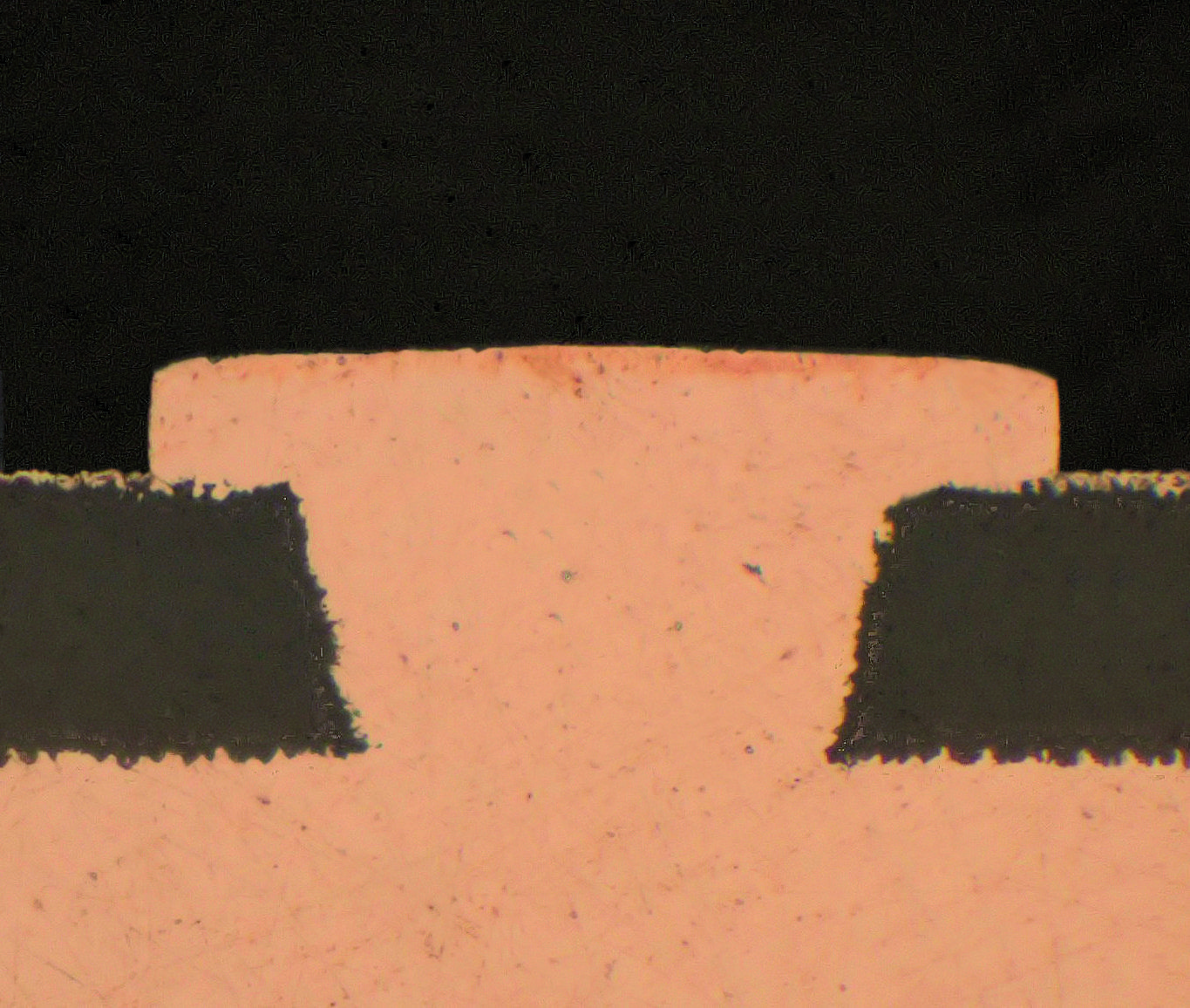
Fig 2: InPro® SAP2
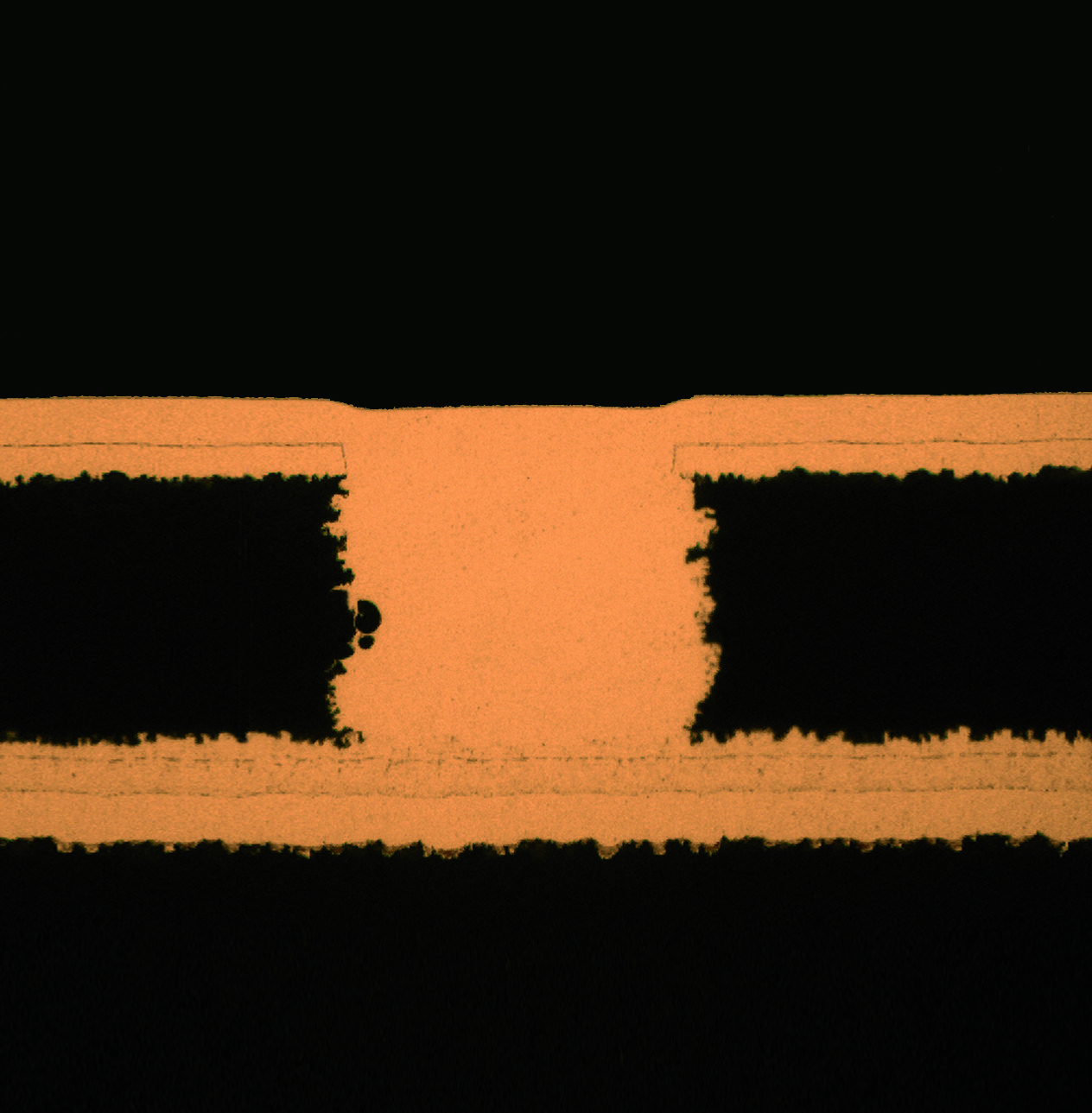
Fig 3: InPro® MVF
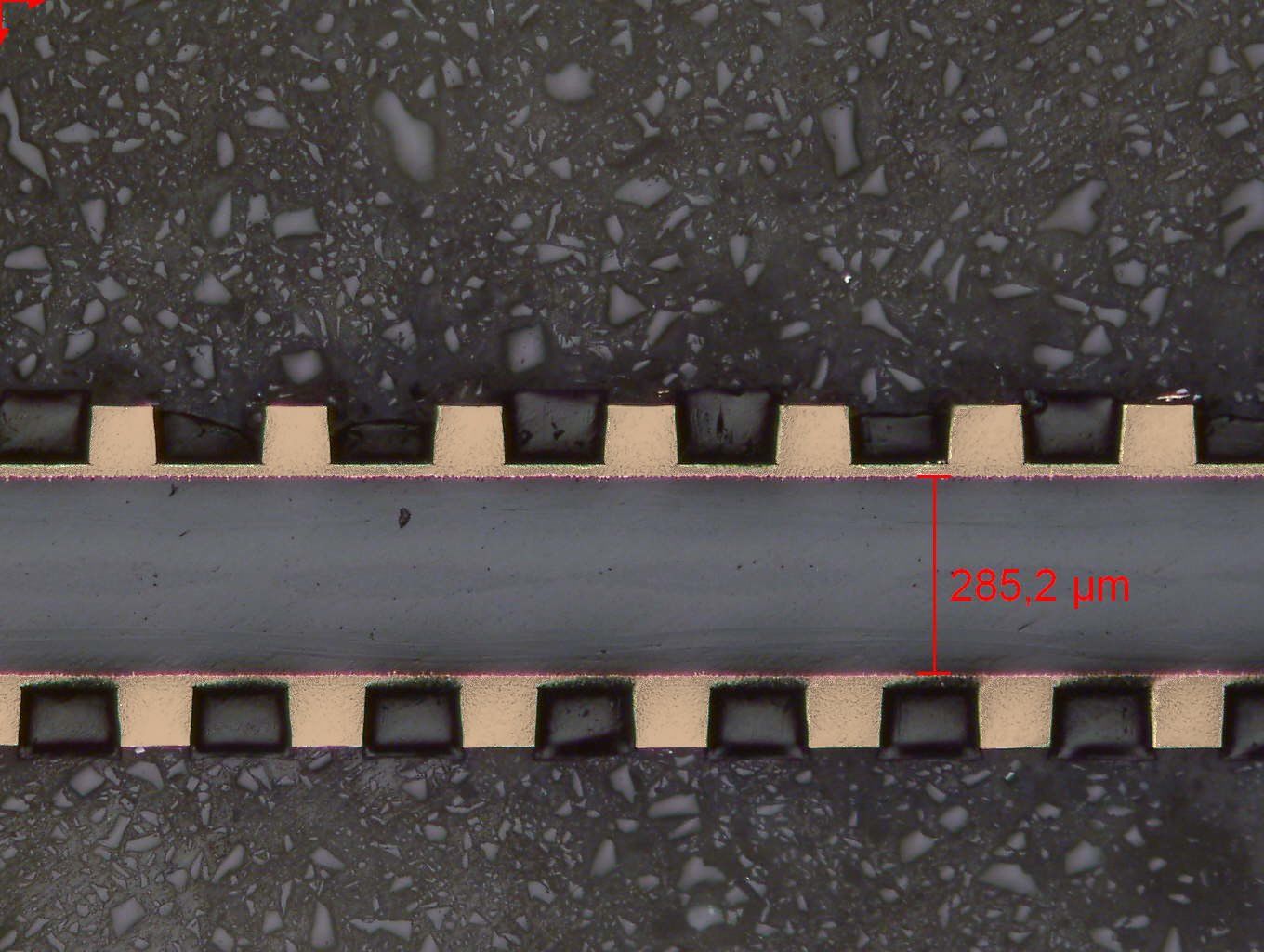
Figure 4: InPro® PI
In the PCB market the packaging density is continuously increasing. The use of blind micro via technology has allowed rapid developments in HDI board manufacturing. The demand for ever rising overall production yields requires high process reliability. Simultaneously the demand for continuous reduction of process costs is always present. That is why PCB manufacturers increasingly run their production with improved automation systems (such as conveyorised plating systems) for mass production. One could summarize that the market demands ever smaller, faster and cheaper solutions.
Chemicals used in PCB manufacturing need to be compatible to the corresponding equipment in order to achieve optimum production results. Needless to say that Vertical Conveyorised Plating (VCP) lines also require specifically designed processes to ensure uniform production conditions. For this specific equipment, Atotech has developed several solutions for plating of copper in order to best serve the needs of the industry.
InPro® series
Atotech’s InPro® series is designed for use with insoluble anodes and direct current (DC) rectification. The processes operate best with equipment using sparger system for electrolyte agitation. Copper replenishment is usually done by copper oxide as external source. Atotech offers solutions for conformal plating, pillar plating and filling of blind micro vias (BMV) and through holes (TH). All processes can also be used in conveyorised systems where strong electrolyte agitation is present.
InPro® THF – vertical pattern through hole filling
InPro® THF was developed for through hole filling application for advanced package substrate technology. The process offers excellent through hole and microvia filling performance, showing lower void size and rate when compared to existing vertical processes in the market. In pattern mode it exhibits an outstanding within-unit distribution, which is a critical factor for the subsequent processing steps. It may be operated in panel mode as well. The process shows stable filling performance over a long bath age. It is one of Atotech’s solutions for BMV filling in (a)mSAP technology.
InPro® SAP2 – vertical pattern BMV filling
InPro® SAP2 was developed for pattern BMV filling applications specifically for advanced package substrate technology. The process shows outstanding filling stability in terms of bath age with over 2,000 Ah production time at a customer without carbon treatment. The filling of BMVs in package substrate dimensions works reliably with a dimple of < 5 µm in combination with an excellent within-unit distribution. The process is suitable for fine line production for existing and next generation substrates.
InPro® MVF – vertical BMV filling for HDI
InPro® MVF is a process for panel and pattern BMV filling for HDI board production. It provides a reliable filling performance with surface thicknesses down to 12 µm copper allowing cost savings in BMV filling production. The process shows no tendencies for necking or dome plating for best subsequent process compatibility. Often there are both through holes and BMV filling on the same panel and InPro® MVF gives very good throwing power in the through holes without corner flattening. The plated copper reliability meets industry standards.
InPro® PI / InPro® CPF – vertical Pillar Plating
Pillar plating is different to common BMV filling. There are tall copper pillars plated on a flat surface (C4 structures) at high current densities and smaller copper posts where filling of recesses is required. The tall copper pillars are defined by photoresist only and are plated bottom up. InPro® PI offers outstanding pillar planarity at high current densities together with outstanding pillar height distribution. InPro® CPF is targeting copper post plating where solder resist recessions have to be filled up. The process is specially designed for improved within-pad uniformity combined with good levelling performance.
InPro® VLF – vertical conformal plating
InPro® VLF was designed to serve the need for reliable conformal plating in equipment with insoluble anodes and high solution turbulence. It provides excellent plating performance in terms of throwing power in both through hole and microvia at high current density. InPro® VLF deposits copper with very good physical properties and shows no signs of corner flattening in through hole plating resulting in excellent reliability results for TCT and solder shocks.
Summary
The Atotech portfolio for plating of copper in VCP lines meets and exceeds market requirements. All InPro® processes are compatible to the different conveyorised systems in the market. With our new processes, we provide the best solutions for the different market needs – no matter if you are looking for conformal, filling, or pillar plating.
For more information, please contact:
Henning Huebner
Global Product Manager Panel and Pattern Plating Atotech Deutschland GmbH
Phone: +49 (0)30 – 349 85 434
Email: henning.huebner@atotech.com
Product highlights
ST-Line®: Atotech’s all new pretreatment line
New cost effective equipment for advanced surface preparation
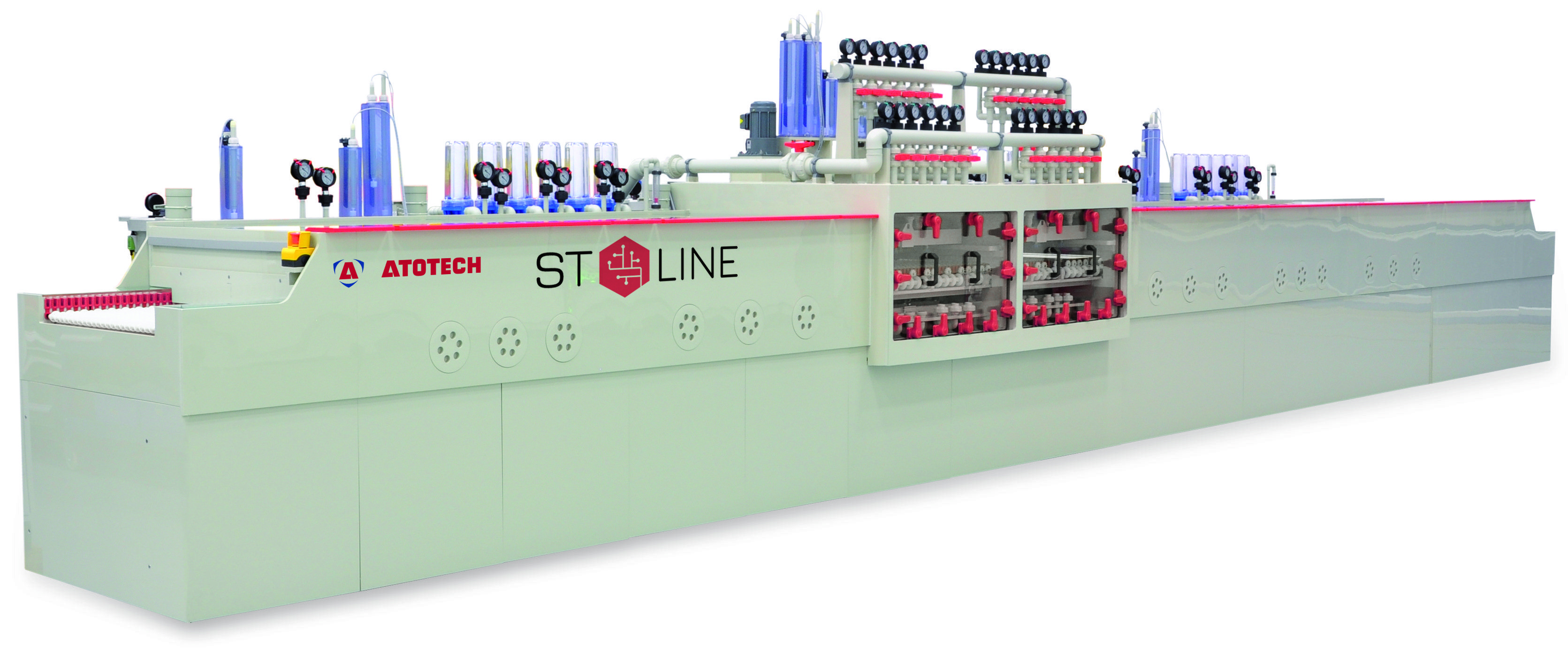
Fig1: Atotech’s new ST-Line®

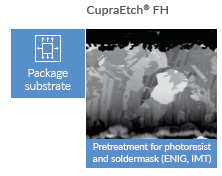
Fig 2: Atotech’s CupraEtch® Family
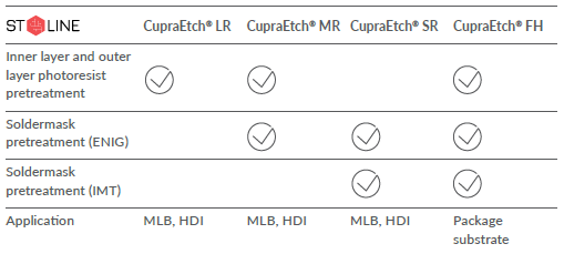
Fig 3: ST-Line® Application
We have developed a new ST-Line®, a state-of-the-art equipment designed for the requirements of soldermask and dry film pretreatment processes in the manufacturing of PCB. We use our high quality and high precision manufacturing capabilities at our new plant in Guangzhou to provide this equipment to the industry. With the accelerated move to finer lines and spaces across PCB applications, we consider it to be an ideal time to introduce ST-Line® in combination with CupraEtch® chemical solutions.
Commenting on the recent launch, Mr. Frank Runkel, Atotech’s Vice President Equipment, stated:
“Atotech is well known in the industry for being the only company to offer chemistry, equipment and processes for PCB manufacturing out of one hand. The introduction of ST-Line® underscores our commitment of delivering not only chemistry or hardware but a full systems solution package to our customers. Engineered and built in our new Guangzhou equipment plant and manufactured on high precision machining tools, the ST-Line® is a high quality product that assures maximum yield at a competitive price. In combination with our CupraEtch® chemistry products the line enables our customers to meet their sustainability goals by reducing their waste water volume measurably.”
ST-Line® and CupraEtch®
The new line is fully compatible with our existing offering of CupraEtch® pretreatment chemistry and is expected to boost yields to control production costs. The two combined form a multipurpose microetch system for the pretreatment and adhesion promotion of primary imaging resists and soldermasks. Our customers can deploy the equipment for inner and outer layer photoresist pretreatment as well as soldermask pretreatment (compatible with all Final finishes, including ENIG and IMT) processes across MLB, HDI and package substrate applications. Superior in quality and design, the line also meets rigorous safety standards.
Features and advantages
Key highlights of our ST-Line® include its ease of operation, intuitive safety controls and fully controlled temperature detection in dryer module.
Key figures:
– Working speed: 2m/min – 4m/min
– Working size: 630 mm x 630 mm
– Core thickness: 0.05 – 2.0 mm
– Module materials: PP, SS/Ti
Benefits to the customers:
– For inner layer, outer layer and soldermask pretreatment
– High quality equipment for best process performance
– Considerably reduced waste-water
– Highest electrical security control and safety standard
– Equipment and chemistry out of one hand
– Industry leading customer service
Backed with our extensive local presence, customers will also have access to our highly trained experts and support through various production stages.
For more information, please contact:
Stephan Hotz
Global Product Manager Surface Treatment Technology
Atotech Deutschland GmbH
Phone: +49 (0)30 – 349 85 534
Email: stephan.hotz@atotech.com
Scott Zhang
Sales and Product Marketing Manager
Atotech (China) Chemicals Ltd.
Phone: +86 20 8297 5160
Email: scott.zhang@atotech.com
Product highlights
Atotech’s EcoFlash® S 200: New differential etching
Advanced & Recyclable Differential Etching
EcoFlash® S 200
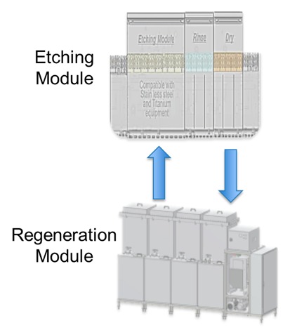
Figure 1: Process Flow and of 1-step Differential Etching product EcoFlash® S 200

Figure 2: Undercut difference between conventional Differential Etching and EcoFlash®
A key new product that was released by Atotech during early 2016 to help IC – Substrate manufacturers improve the performance in the Differential Etching productions step is EcoFlash™ S 200. This ferric sulfate based etchant runs in parallel with a recovery unit which allows for solution regeneration and copper recycling, as can be seen in Figure 1. The simple one-step and low-temperature process is unique and specially designed to maintain the conductors undercut-free and in their original shape. Thus, EcoFlash™ S200 is able to improve yields, enable lower line/space manufacturing and significantly reduce the use of chemicals.
Since its introduction the process has attracted widespread market attention, most notably for its clear benefits over currently employed sulfuric acid / hydrogen peroxide Differential Etching systems.
A main drawback of most none-peroxide based etching solutions is the fluid dependent etching characteristics. Highly agitated areas are etched faster than slowly agitated ones. We implemented the Rotating Disk Electrode (RDE) as a tool to simulate etchant agitation influences in a well-controlled environment and to provide highly accurate and precise results. In contrast to peroxide based etchants the additive free iron(III)-based etching solution is highly affected by the solution agitation. By adding the EcoFlash® S200 additive package to the iron(III) etchant it’s performance dramatically changed. The etch rate becomes completely independent of the rotation speed and hence the mass transport of the iron(III) to the surface is uniform controlled by a diffusion layer build up by the EcoFlash® S200 additive.
Besides flow differences, peroxide and iron based etchants differ in undercut formation especially in fine line areas. This kind of over-etching is significantly pronounced for hydrogen peroxide based systems. Compared to this, the undercut for EcoFlash® S200 remaines on a negligible level and allows a complete removal of the seed layer while ensuring the interfacial integrity and mechanical stability of the conductors.
Peroxide based etchant resulted in undercut formation, which leads to a separation between conductor and dielectric material due to a loss in adhesion. Furthermore, a severe line width reduction will be obtained, as can be observed in Figure 2.
In contrast to this, EcoFlash® S200 kept the interfacial integrity while the seed layer was completely removed and ensured the differential etching capability for future packaging substrates.
This clear advantage has also become visible when testing our product for a Japanese customer who had the direct request to evaluate our EcoFlash® S200 for dense and isolated conductors, in this case conductors with L/S 12/12 µm and L/S 12/50 µm. Due to the nature of hydrogen peroxide etchants and their plated copper and undercut attack creating isolated conductors, the customer currently has to plate significantly more copper in order to create an isolated conductor vs a dense one. This results in an undesirable waste of plated copper, which the customer would like to avoid. Looking at the customer sampling results in Figure 3, we can see that EcoFlash® S200 shows equal undercut and line width reduction for both, dense fine lines and fine-line isolated conductors.
With these excellent results and clear benefits versus currently used etchants the new EcoFlash® S200 has attracted widespread market interest and is currently under focused evaluation at several key customers in Japan and Taiwan.
For more information, please contact:
Stephan Hotz
Global Product Manager Surface Treatment Technology Atotech Deutschland GmbH
Phone: +49 (0)30 – 349 85 534
Email: stephan.hotz@atotech.com
Product highlights
Atotech’s Booster MR: New adhesion enhancement
Direct Plating on Molding Compounds for Package Level EMI Shielding
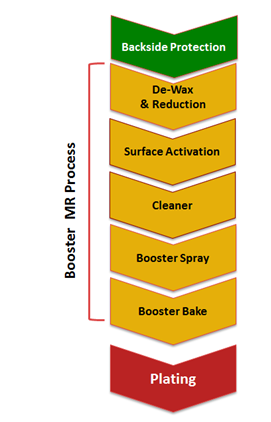
Figure 1: Process flow logic of Booster MR adhesion promoter for plating on molding compound for EMI Shielding

Figure 2: Cross-hatch tape test results on various plated metal options plated after new chemical pretreatment
Plating on molding compound is a relatively new field which is opening up new package designs. One major application is conformal EMI shielding (package level shielding) of ICs. A popular method to provide a metallic seed layer for “Conformal Self EMI Shielding” is sputtering and conductive paste. However this method has very high costs and it has the technical drawbacks of poor sidewall coverage and limited metal layer thicknesses that would not meet requirements for lower frequency noise shielding. Classical electroless and electrolytic plating metallization are much more desirable but have been so far limited by insufficient adhesion by existing chemical pretreatments.
Booster MR
To overcome these limitations Atotech introduces a new chemical treatment process, Booster MR. The Adhesion Enhancement process follows the process flow outlined in figure 1.
In a first step the backside circuity is protected, usually using Nitto tape. Then a dewax step is applied to provide wettability on the molding compound surface. This is followed by a surface activation and cleaning step. Finally the Booster MR chemical adhesion promoter is applied in spray mode and the process is finalized by a baking step.
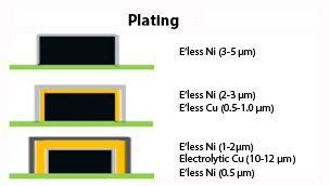
The surface is then passed into the standard plating process where it is seeded with Pd activator for electroless and electrolytic, copper or nickel plating. The thickness of those layers is typically on the order of several microns for EMI shielding applications. The exact sequence and thickness depends on the specific shielding requirement.
For internal testing we used a tape test to measure adhesion performance and the results are shown for three common plating conditions (see figure 2 for cross-hatch test results).
Market Introduction
Atotech is currently rolling this new process out to the market. Testing and sampling is available from select TechCenters in Asia. Also, further evaluation and results such as dicing & peel strength tests, shielding effectiveness measurements and further investigations into manufacturing benefits are available with Atotech upon request.
For more information, please contact:
Stephan Hotz
Global Product Manager Surface Treatment Technology Atotech Deutschland GmbH
Phone: +49 (0)30 – 349 85 534
Email: stephan.hotz@atotech.com
Product highlights
Automotive market leader: Stannatech® 2000
The only immersion tin process that combines cost with reliability
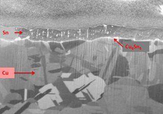
Figure 1: Soldering immersion tin – FIB of an as received pad
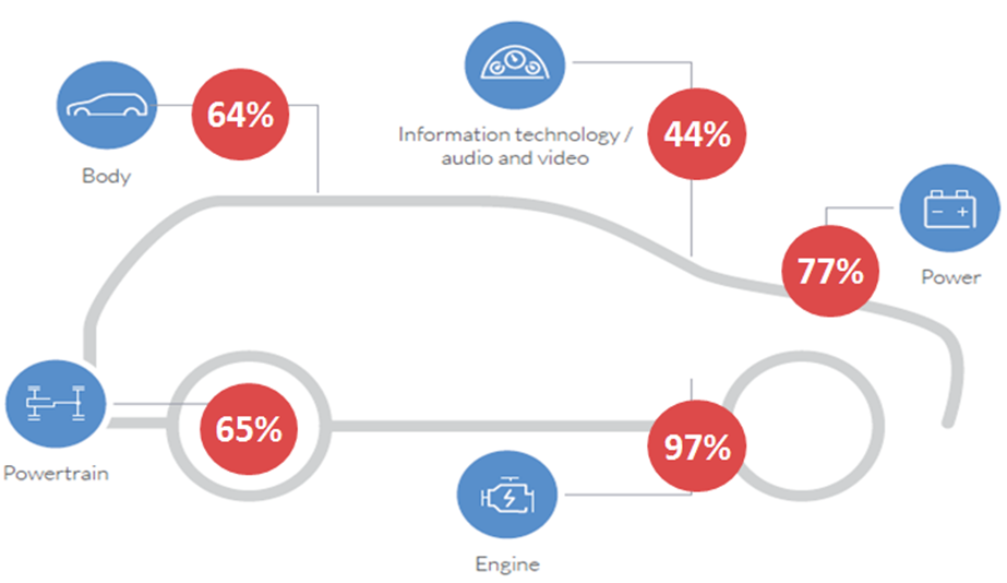
Figure 2: The presence of Atotech’s Stannatech® in the segments of a car

Figure 3: Representation of Stannatech ® 2000 according to automotive segments versus top five automotive OEMs
Atotech’s Stannatech® 2000 is the most production represented immersion tin on the market with over 70% market share and more than 135 customers. The key to this success is a system approach that fuses high end equipment with optimized utility chemistry which is able to meet deposition rates enabling unique equipment footprints. It also out performs all other final finishes with regards to highly corrosive environmental testing.
Automotive Industry
The stimulating impact of the automotive industry has sharpened focus on immersion tin (Stannatech® 2000) more than ever before. In an environment dominated by reliability, the automotive market not only has very stringent specifications but also demands thorough qualification protocols. Qualification is ultimately a costly exercise. The good news is that Stannatech® 2000 is already qualified by many tier one OSATs.
Stannatech® 2000 is already established as the POR final finish for most of the automotive industry. It is present in many of the top 30 automotive PCB manufacturers and in 80% of the top 10 end users.
Safety and technical capabilities
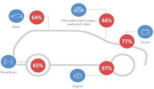
Safety and the technical capabilities are important considerations in the automotive electronics industry. The production volume that can be attributed to Stannatech® 2000 according to the application segments, as defined by DENSO (Engine, power train, body, IT/AV and power), definitively highlights the domination of Atotech’s I-Sn in all areas other than infotainment. This is demonstrated in figure 2, where in the engine segment Stannatech corresponds to 97% of the m² production.
Figure 3 is a representation of Stannatech® 2000 at the top 5 automotive OEMs for each segment. It is evident that Stannatech® 2000 is utilized for high reliability automotive applications such as engine CPUs, braking and air bags.
Intensifying safety legislation is ensuring that electronically controlled systems become state of the art. Having established the relationship between reliability and i-Sn, the future for Stannatech continues to be bright.
In the global arena Stannatech is being applied vertically and horizontally. The systems approach is still championed by Atotech and system sales continuously increase over the years.
Ultimately, Stannatech® 2000’s market share equates to a production volume of over 10 million m² per year.
For more information, please contact:
Rick Nichols
Global Product Manager Surface Finishing Atotech Deutschland GmbH
Phone: +49 (0)30 – 349 85 340
Email: rick.nichols@atotech.com
Trade show news
Global events and trade shows
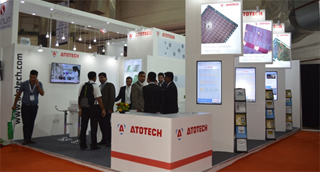
Atotech booth at the IPCA 2016
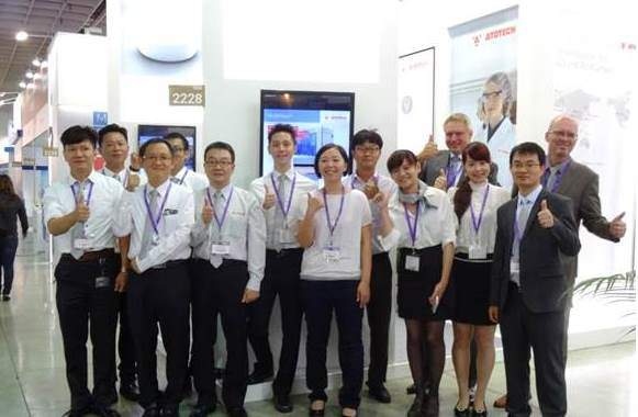
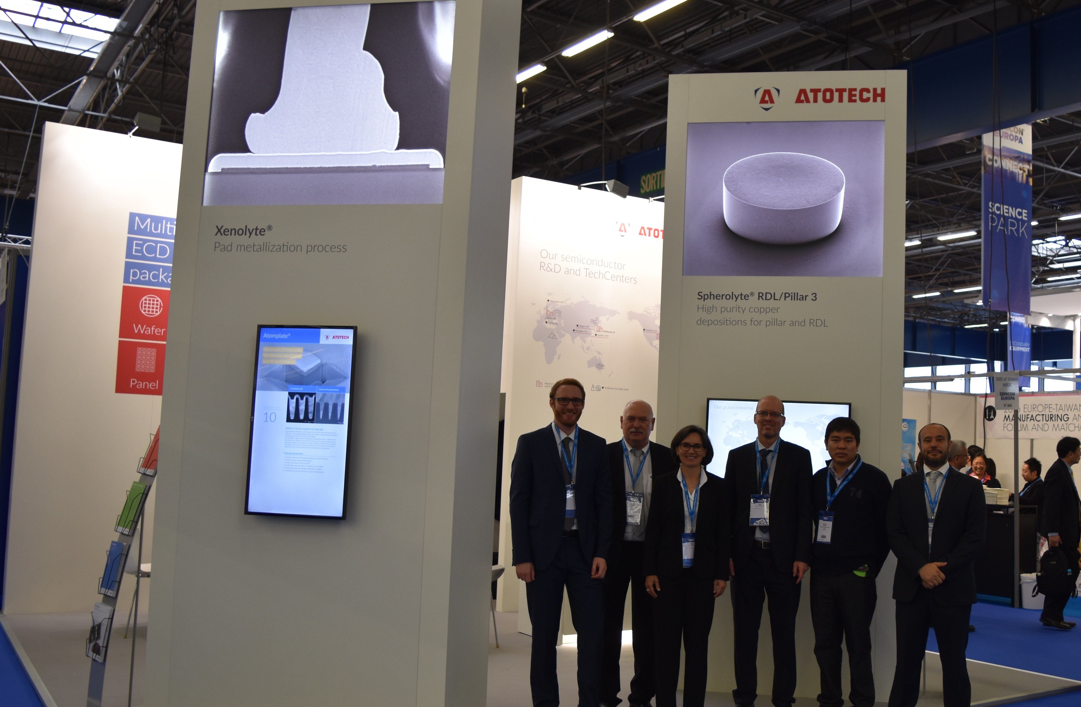
Atotech’s team at the Semicon Taiwan
Atotech Team at the Semicon Europa 2016
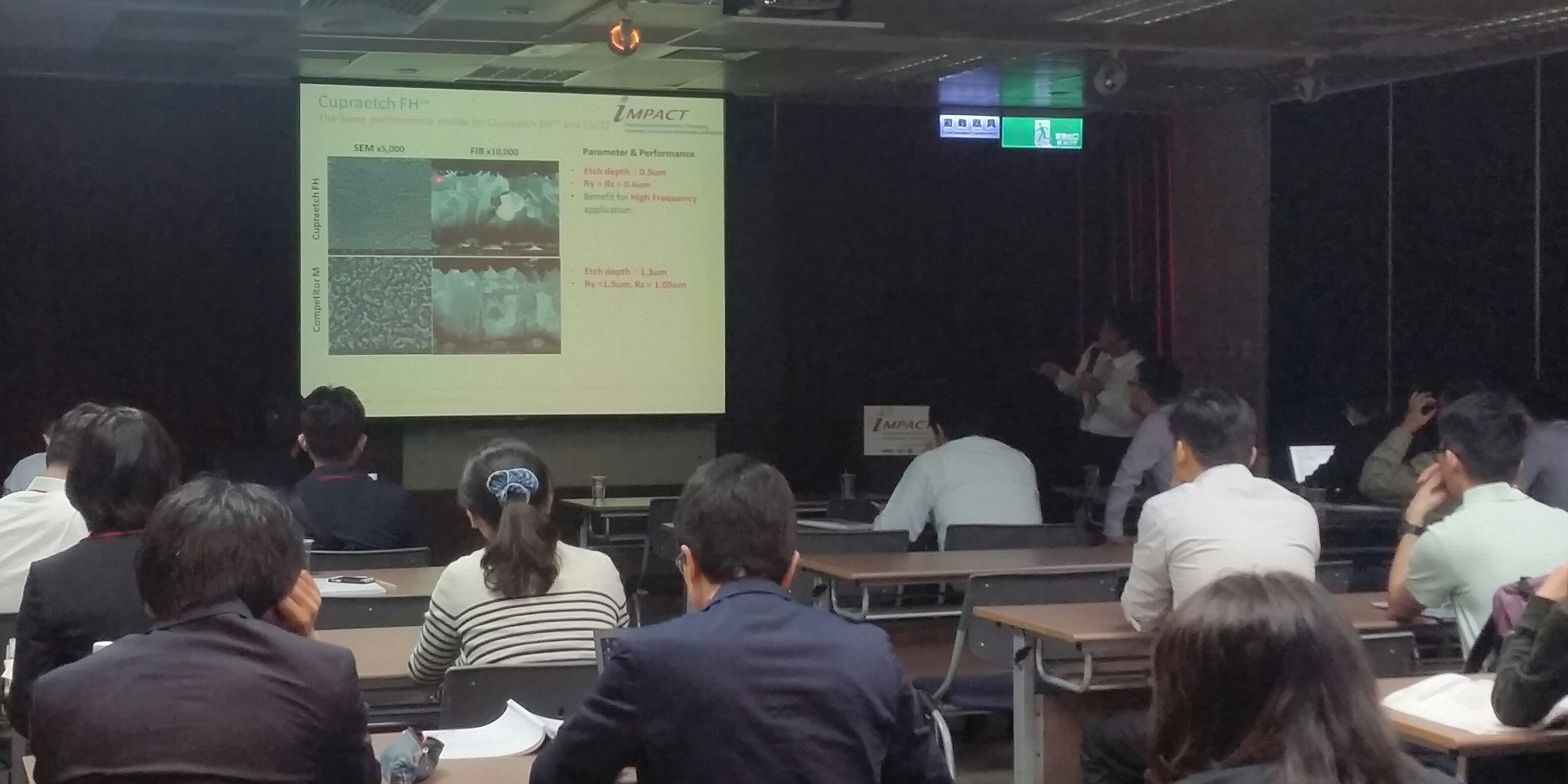
Wonjin Cho’s presentation on CupraEtch FH at the TPCA IMPACT 2016
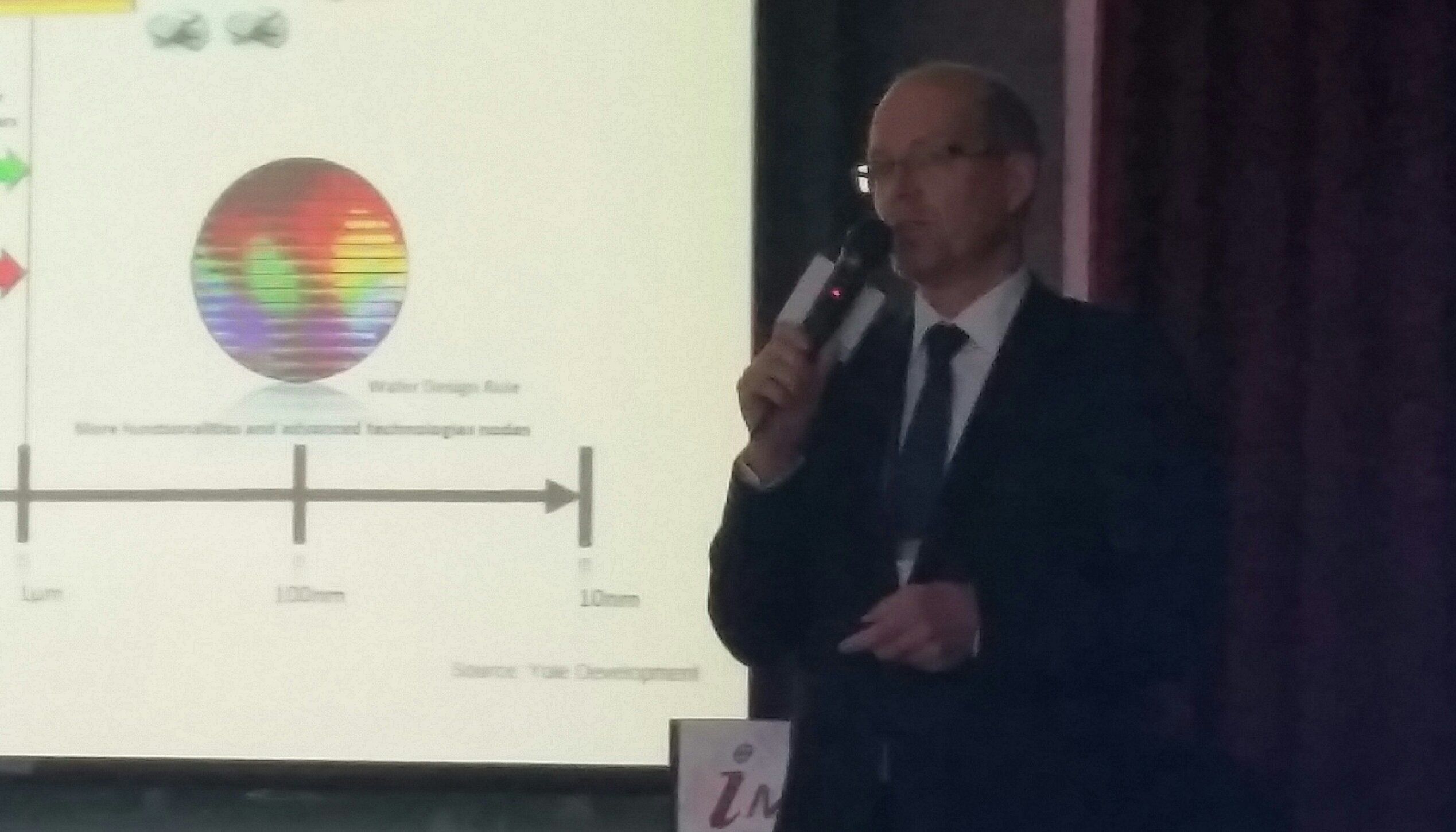
Bernd Roelfs on MultiPlate at TPCA IMPACT 2016
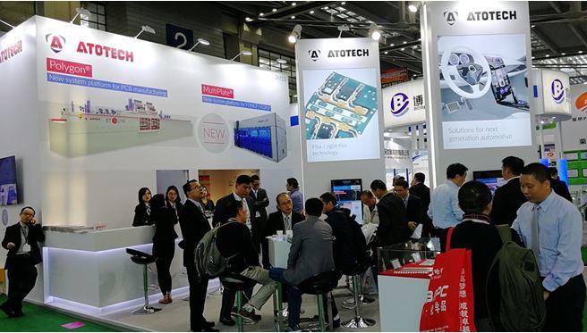
Atotech’s booth at HKPCA & IPC Show 2016
Past Events
Atotech participated in a number of key global events during the past few months. Here’s a quick highlight:
IPCA Expo 2016
The IPCA Electronics Expo 2016, organised by the India Printed Circuit Association (IPCA), was held from August 17 to 19, 2016, in New Delhi, India. The Indian electronics industry is poised for significant growth, owing to an enormous demand in the domestic market and an ongoing paradigm shift to building an end-to-end manufacturing ecosystem. This growth is being encouraged by policies like ‘Make in India’, fiscal incentives and by promoting FDI. The IPCA was organised to offer a common platform to all major stakeholders in the electronics industry to share and collaborate towards Indian electronics landscape. It provided the opportunity to gain insights into the latest technologies and applications in all electronics sectors.
Over 128 Exhibitors exhibited more than 250+ brands to about 8,300 visitors. Many new and prospective as well as existing customers visited our Atotech booth in order to learn more about our diverse product portfolio, such as our semiconductor product portfolio, Ecopact® CP E – our cost effective solution for green multilayer production -, Aurotech® Plus, or Bond Film® MS 800, our new oxide replacement process.
SEMICON Taiwan 2016
SEMICON Taiwan 2016 – the premier event in Taiwan for microelectronics manufacturing – took place from September 7 to 9, 2016, at the Taipei Nangang Exhibition Center in Taipei, Taiwan. With more than 30,000 visitors and 600 exhibitors, the show focused on high tech facilities and precision machinery, smart manufacturing, secondary markets, and CMP, among others. At our booth, senior leaders and experts talked about our new offerings and innovations, such as our newly launched MultiPlate® tool – An ECD tool for next generation packaging technologies.
Atotech’s presentations on “MultiPlate® – An innovative ECD system for next generation packaging technologies” and on “Spherolyte® UF3 for High Speed Pillar Plating” at the corresponding conference “TechXPOT” were well received. Thomas Beck’s (Global Business Manager for Semiconductor Advanced Packaging) speech at the Materials Forum on “Atotech’s sustainable production methods and technology solutions for the semiconductor industry” – explaining our expertise and leading knowledge in sustainability – also drew much attention.
SEMICON Europa 2016
Atotech presented and showcased at the SEMICON Europa 2016 in Grenoble, France, from October 25 through 27, 2016. SEMICON Europa is a leading exhibition in Europe for the semiconductor industry. At its booth, Atotech’s semiconductor experts discussed the latest additions to our portfolio as well as our recently introduced MultiPlate tool. The featured portfolio included high purity plating chemistries for electroless and electrochemical applications from dual damascene processes to advanced packaging processes such as copper pillar, RDL, and pad metallization.
At the adjacent Power Electronics Conference, Markus Hoerburger, Assistant Product Manager Semiconductor Advanced Packaging at Atotech Deutschland GmbH, introduced our MultiPlate® with a presentation on “Innovative plating system for an embedded packaging concept of power modules”. The presentation explained the innovative double sided Cu plating concept that was developed during the European EMPower project.
The three day show was a full success for Atotech, with interesting discussions and many booth visits from customers, key companies, partners and interested passers-by.
TPCA & IMPACT Taiwan 2016
Atotech exhibited and presented at this year’s TPCA Show 2016, which was held in conjunction with IMPACT-IAAC 2016, from October 26 to 28 at Taipei Nangang Exhibition Hall in Taipei, Taiwan. IMPACTs theme was “IMPACT on the Next Big Things” with the Internet of Things being a major theme again this year. As every year, the show was a great platform to meet global PCB and advanced packaging experts and to discuss new ideas and innovations at Atotech’s booth. Atotech specialists shared their expert knowledge in two presentations during the three day show.
During the Advanced Materials session of TPCAs IMPACT Conference, Wonjin Cho (Product Development Manager for Surface Treatment Technology) introduced the audience to the latest addition to the CupraEtch® family of adhesion promoters: “CupraEtch® FH”. CupraEtch® FH targets HDI and multilayer applications and creates a unique structured surface ideal for adhesion of soldermasks. Unlike competitive and generic systems, CupraEtch® FH creates its outstanding adhesion with a low etch depth, offering immediate benefits especially in soldermask applications where reduced etching is desirable to control critical dimensions while maintaining performance with Immersion Tin and ENIG finishes.
Later on, Bernd Roelfs (Global Product Manager for Semiconductor Advanced Packaging) brought a packed room up to speed on the new Multiplate® tool for Wafer and Panel Level Packaging. Using optimized fluid delivery and unique electrolytes, Multiplate® offers high throughput RDL and Cu pillar plating on wafers with a minimal Cost of Ownership. With a simple change, the tool can be converted from a wafer to panel format machine, ensuring product flexibility and future proofing, should the market adopt this desirable and heavily discussed format. Multiplate® is unique in the market and generated a lot of interest in this busy session.
HKPCA & IPC Show 2016
The International Printed Circuit & APEX South China Fair 2016 (HKPCA & IPC Show) ran from December 7 through 9, 2016, in Shenzhen, China. As one of the world’s most influential trade shows for the Printed Circuit Board and Electronic Assembly industry, the show focused on “Global Wisdom Shaping the Future”. One of the main topics was the automotive market, since it is the fastest growing segment in the PCB market, with a worldwide growth forecast of 6% in 2016. The more than 2,500 booths from around 550 exhibitors displayed the latest and most creative industry offerings, with close to 100 exhibitors showcasing for the first time at the show.
Atotech’s booth presented our latest technology and cutting-edge new products, such as our InPro® family for vertical conveyorized systems, our MultiPlate® plating tool, or our brand new ST-Line® for advanced surface preparation. Experts and senior leaders were happy to discuss our product portfolio, latest technology and market trends, as well as future developments with visitors and passers-by.
Future Events
Meet our experts and senior leaders at key global events coming up around the world:
Internepcon Japan 2017
Date: January 18 – 20, 2017
Venue: Tokyo Big Sight, Japan
SEMICON Korea 2017
Date: February 08 – 10, 2017
Venue: COEX Seoul, Korea
IPC / APEX Expo 2017
Date: February 14 – 16, 2017
Venue: San Diego Convention Center, USA
CPCA Show 2017
Date: March 07 – 09, 2017
Venue: National Exhibition and Convention Center Shanghai, China
SEMICON China 2017
Date: March 14 – 16, 2017
Venue: Shanghai New International Expo Center, China

Industry News
Market and Technology
At a glance report of all the important market and technology News you can’t miss
Fan-Out Wafer Level Packaging Takes Off
Fan-Out Wafer Level Packaging (FOWLP) has become the hot topic for the semiconductor industry as it offers numerous performance and cost advantages in terms of smaller form factor, thinner package, higher I/O density, multi-die solutions, and more. What sets the FOWLP apart from package-on-package (POP) form factors found, for example, in earlier generations of iPhones, are thinner packaging profile, higher I/O counts, better electrical and thermal performance, and yet a better cost structure. This is clearly a game changer of the packaging industry, with Apple/TSMC setting the tone for a packaging trend in the mobile market and it’s clear that almost all the other major OSATs, as well as some IDMs are planning their versions of fan-out packaging. Going forward, we will see more FOWLP implementation in packaging baseband processors, PMIC, GPU, and RF devices in mobile devices and wearable products. FOWLP also has the potential extending to CPU, GPU, FPGA packaging for high-performance computing.
Source: http://www.semi.org/en/fan-out-wafer-level-packaging-takes
Let’s twist again: new flexible lithium-ion battery
The Japanese company Panasonic Corporation announced that it has developed a flexible lithium-ion battery with a thickness of only 0.55mm, or about 0.022 inches. The battery has demonstrated that it retains its characteristics during bending and twisting tests. This battery can maintain more than 99% of its initial capacity after 1,000 bends with a radius of 25mm, or after twisted 1,000 times with an angle ±25°/100mm, thanks to a newly developed laminated outer layer and newly developed internal structure.
Source: http://www.advancedsciencenews.com/lets-twist-again-new-flexible-lithium-ion-battery/
PCB makers hike prices due to increased CCL cost
In response to price hikes by CCL (copper-clad laminate) suppliers, Taiwan-based PCB makers have raised their quotes to reflect increased costs. Prices for copper foil have significantly risen because makers have increased supply of more profitable copper foil used to produce lithium batteries for use in electric vehicles in the China market. PCB price hikes have increased costs for PC and smartphone vendors.
Source: http://www.digitimes.com/news/a20161121PD203.html
Nan Ya Printed Circuit Board to sell entire stake in two firms
Nan Ya Printed Circuit Board Corp. announced it will sell its entire 4.6 million shares of petrochemical firm for T$ 460.6 million and its 5.4 million shares of chemical fiber firm for T$ 516.9 million. It will hold no stakes in the two firms after selling.
Source: http://www.reuters.com/article/idUSL4N1DM2OK
For first time, carbon nanotube transistors outperform silicon
For the first time, engineers have created carbon nanotube transistors that outperform state-of-the-art silicon transistors. The research team’s breakthrough could pave the way for carbon nanotube transistors to replace silicon transistors, and is particularly promising for wireless communications technologies.
Source: http://electroiq.com/blog/2016/09/for-first-time-carbon-nanotube-transistors-outperform-silicon/
Researchers Build World’s Largest Database of Crystal Surfaces and Shapes
The University of California at San Diego and Lawrence Berkeley National Laboratory have created an open source database of elemental crystal surfaces and shapes. Called Crystalium, the database can help researchers design new materials for various applications, such as batteries, catalytic converters, fuel cells, semiconductors and others. Crystalium provides data on surface energies and equilibrium crystal shapes of more than 100 polymorphs of 72 elements in the periodic table.
Source: http://ucsdnews.ucsd.edu/pressrelease/researchers_build_worlds_largest_database_of_crystal_surfaces_and_shapes
NTU develops energy saving filters for wastewater treatment
Typically, for the last steps of water purification in a wastewater treatment process, an ultrafiltration (UF) membrane filters out small particles before a reverse osmosis (RO) membrane is used. However, NTU’s proprietary nanofiltration (NF) hollow fibre membrane does away with both ultrafiltration and reverse osmosis, combining the two processes. It also requires only 2 bars of water pressure. Yet it produces water that is almost as pure as through reverse osmosis. This breakthrough technology was developed by NTU’s Nanyang Environment and Water Research Institute (NEWRI) and is now being commercialized by an NTU spin-off company De.Mem. De.Mem will test the new membrane modules in real world usage in its plants to verify its effectiveness and efficiency before scaling up to a full industrial production line.
Source: http://media.ntu.edu.sg/NewsReleases/Pages/newsdetail.aspx?news=84aa55bb-a88e-4eb9-a12e-5dad0884ccbe
Sharp president confirms in speech that Apple will be shifting to OLED displays
Sharp President Tai Jeng-Wu has confirmed that Apple will transition to OLED displays over time. The next generation flexible OLED displays will allow Apple to invent iPhone displays that are curved or iPhones that could fold.
Source: http://www.patentlyapple.com/patently-apple/2016/10/sharp-president-confirms-in-speech-that-apple-will-be-shifting-to-oled-displays.html
Samsung says to invest USD 296 million to expand India plant
Samsung Electronics Co. Ltd. will invest USD 295.83 million to expand its plant in northern India, according to the company. The plant in Noida, near New Delhi, makes mobile phones, refrigerators and television.
Source: http://in.reuters.com/article/us-samsung-elec-india-idINKCN12I0BX
A new age of smart manufacturing underway
SEMI estimates that by 2020, about one billion IoT devices will be at work in manufacturing facilities and global manufacturers will invest around USD 70 billion in IoT solutions that year, up from USD 29 billion in 2015. The goal is that product design data and manufacturing state data will travel through the manufacturing process with the product.
Source: http://electroiq.com/blog/2016/07/a-new-age-of-smart-manufacturing-underway/
Automotive Relay Market size worth USD 14.5 billion by 2023, with 6.5% CAGR estimations from 2016 to 2023: Global Market Insights Inc.
Rapid technological innovation is anticipated to drive automotive relay market size from 2016 to 2023. This is due to the evolution of automobile electronics from simple switches to high-frequency signals on microwave and millimeter-wave. Enhanced driving experience and substantial safety offered by these devices are expected to propel the automotive relay market.
Source: http://globenewswire.com/news-release/2016/07/19/857185/0/en/Automotive-Relay-Market-size-worth-USD-14-5-Billion-by-2023-with-6-5-CAGR-estimations-from-2016-to-2023-Global-Market-Insights-Inc.html
Global flexible electronics market will grow during 2016-2020 following the arrival of bendable Smartphones
Technavio analysts forecast the global flexible electronics market to grow at a CAGR of close to 67% during 2016 to 2020. Especially the following four factors are contributing to the growth of the global flexible electronics market: capacity expansion plans, growing demand for wearables, increase in the number of application segments, and the incorporation of printed batteries in mobile devices.
Source: http://www.businesswire.com/news/home/20160829005398/en/Global-Flexible-Electronics-Market-Grow-2016-2020-Arrival
Taiwan Printed Circuit Board Techvest to buy back 5.5% stake for T$ 7.05 billion
Taiwan Printed Circuit Board Techvest says it will repurchase 15 billion shares of its common stock, a 5.5% stake, until November 11, 2016. The total share repurchase consideration is T$ 7.05 billion.
Source: http://www.reuters.com/article/idUSL3N1BO315
AT&S offers comprehensive solutions for miniaturization on all interconnection layers
The “AT&S Toolbox” provides a vast range of high-end technologies that can be combined with each other for miniaturization on all interconnection layers. It uses technologies such as IMS, multilayer, HDI, and any layer, and allows for conductor track widths/spacing of 15µm as well as significantly less than 10µm for IC substrates, among others.
Source: http://www.iconnect007.com/index.php/article/100078/ats-offers-comprehensive-solutions-for-miniaturization-on-all-interconnection-layers/100081/?skin=pcb
Electronic circuits printed at 1 micron resolution
A research team developed a printing technique capable of forming metal circuits with line width being 1 µm on flexible substrates, thereby forming minute organic TFTs which operate at a practical level. Future studies will aim at applying this technique in various fields such as large-area flexible displays and sensors.
Source: http://www.nanowerk.com/nanotechnology-news/newsid=44338.php
Chinese researchers created a safe method to recycle PCB’s
PCBs can now be recycled in a way that is less damaging to the environment. Chinese researchers have developed a technique that allows for the recovery of valuable metals without releasing toxic fumes. With their technique, metals can be recovered by vacuum fractional distillation, while non-metal components can be compressed into plaques for use as construction material.
Source: http://knowtechie.com/chinese-researches-created-a-method-to-recycle-pcbs/
World’s first 3D printed plane unveiled
European aerospace company, Airbus, has created a mini-plane, named Thor (“Test of High-tech Objectives in Reality”), which is the world’s first 3D printed aircraft. The windowless drone weighs around 21 kilograms and is less than four meters long. The aircraft is completely 3D printed and able to fly.
Source: http://www.dailymail.co.uk/sciencetech/article-3627187/World-s-3D-printed-plane-unveiled-Airbus-windowless-Thor-aircraft-pave-way-cheaper-faster-flights.html
Liquid glass: Casting glass like cement
A team at the Karlsruhe Institute of Technology (Eggenstein-Leopoldshafen, Germany) has now introduced “Liquid Glass” (LiqGlass), a viscous free-flowing, photocurable nanocomposite containing amorphous silica which can be structured by room-temperature replication using soft molds made from polydimethylsiloxane (PDMS). The cured LiqGlass is then converted to dense high-quality solid glass via thermal debinding and sintering. The resulting glass is chemically and physically identical to commercial fused silica glass. Using LiqGlass it is possible to convert arbitrary physical objects made from almost any material with feature sizes in the range of tens of micrometers and roughness of a few nanometers into glass rapidly and conveniently.
Source: http://materialsviews.com/liquid-glass-casting-glass-like-cement/
Smart sutures send wireless status reports from wound sites
A team of researchers from Tufts University has taken flexible electronics to their next logical step, embedding them in sutures that can monitor the body from the site of the stitching and broadcast their findings to a Bluetooth-enabled device. The stretchable polyurethane threads are covered with carbon nanotubes. In studies, they were able to collect data on their surroundings, including pressure, stress and temperature at the suture site. The threads were attached to a circuit board that measured about the size of half a credit card. The board was able to send data to a smartphone and a computer.
Source: http://newatlas.com/smart-sutures-tufts/44402/
Graphene composite enables metre-sized flexible display
Researchers in Exeter devised a graphene composite – GraphExeter – that is highly conducting. The first prototype was demonstrated in an electroluminescent device, showing its feasibility for luminescent textiles and flexible displays. The extremely low sheet resistance means that screens several square meters in size are now feasible.
Source: http://nanotechweb.org/cws/article/tech/65654
Qualcomm is said to be in talks to buy NXP Semiconductors
Qualcomm is in discussions to buy NXP Semiconductors. If completed, the deal could be valued at more than USD 30 billion. It confirms that connected cars will be one of the most important markets for the electronic industry in the next few years. NXP is making most of its sales from automotive, secure identification solutions, and secure interface and infrastructure sectors, which represent 72% of the total revenue of the company. NXP is, after last year’s acquisition of Freescale, the biggest provider of car electronics.
Source: http://www.nytimes.com/2016/09/30/business/dealbook/qualcomm-is-said-to-be-in-talks-to-buy-nxp-semiconductors.html?_r=0
Global power electronics market expected to witness 6.2% CAGR during 2016- 2022
According to P&S Market Research the global power electronics market was valued at USD 12,872 million in 2015 and is expected to witness a CAGR of 6.2% during 2016 to 2022. Based on technology, the power electronics market generated highest revenue from non-isolated DC-DC segment in 2015. Geographically, Asia-Pacific was the largest contributor to the global revenues of power electronics market.
Source: http://www.psmarketresearch.com/press-release/power-electronics-market
Digitimes Research: Taiwan top-3 foundries see combined revenues rise in Q3 2016
Combined revenues of Taiwan’s top-3 foundries – Taiwan Semiconductor Manufacturing Company (TSMC), United Microelectronics (UMC) and Vanguard International Semiconductor (VIS) – are estimated to be USD 9.36 billion in the third quarter of 2016, up 14.3% sequentially and 18.5% on year, according to Digitimes Research. A seasonal pick-up in end-market demand led to the sequential increase. Meanwhile, revenues saw a substantial on-year growth due to the low point during the same period in 2015. Taiwan’s top-3 foundries saw their combined revenues reach USD 8.19 billion in the second quarter of 2016, up 10.7% sequentially and 1.2% on year. It was also the first after five consecutive quarters of sequential decreases. Revenues generated from 16 nm process technology are estimated at USD 1.75 billion in the third quarter, up 60.6% on quarter. Digitimes Research credited the significant rise to robust shipments for high-end smartphones rolled out by Apple, Huawei and other brands.
Source: http://www.digitimes.com/news/a20161018VL200.html
China to produce 3D NAND chips as early as end-2017
Yangtze River Storage Technology (YRST) will start operating China’s first 12-inch fab for the manufacture of NAND flash and DRAM memory at the end of 2016, and is expected to produce the region’s first homegrown 3D NAND flash memory a year later. YRST will be able to make 32-layer 3D NAND flash chips as early as end-2017. Construction of YRST’s 12-inch fab will be in three phases, with investment totaling USD 24 billion.
Source: http://www.digitimes.com/news/a20161017PD204.html