
Printoganth® P2
Universal high throw horizontal electroless copper process suitable for advanced dielectrics found in “5G” and flex PCB applications
Successor to Printoganth® P Plus
Printoganth® P2 is the latest member of the market leading Printoganth® P series
Superior coverage and adhesion
Printoganth® P2 features excellent, blister-free coverage on both regular and advanced dielectrics
Secure metallization of TH and BMVs
Combines an outstanding throwing power and a compatibility with a wide range of via fill electrolytes
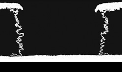
>80% Throwing Power with Printoganth® P2 100×65um BMV
Printoganth® P2
Universal high throw horizontal electroless Copper process suitable for advanced dielectrics found in “5G” and flex PCB applications.
Dielectric adhesion and coverage
Printoganth® P2 has excellent adhesion with no blistering on even the smoothest substrates. Its wide compatibility with multiple dielectric systems makes Printoganth® P2 the ideal choice for manufacturers who have a broad product mix (MLB, HDI, FPCB) or produce mixed dielectric PCBs.
Excellent throwing power
The enhanced stabilizer package in Printoganth® P2 enables an outstanding throwing power into through holes and blind micro vias. Together with its proven compatibility with a wide range of via fill electrolytes, Printoganth® P2 is the ideal solution for challenging HDI PCBs and high aspect ratio panels.

- Universal horizontal electroless copper process for regular and advanced dielectrics
- Multi layer or HDI PCBs using advanced materials such as high Tg FR4, BT, low df/dk materials
- FPCB or Rigid-Flex PCBs
- Panels with high aspect ratio through holes or blind micro vias
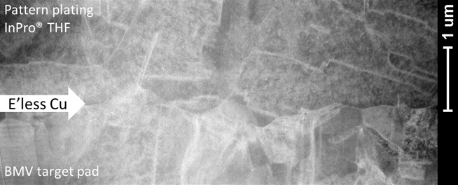
High-angle annular dark-field (HAADF)-TEM investigation at a BMV target pad showing excellent, void-free Cu to Cu interconnection
- Outstanding adhesion and non-blistering characteristics, even on challenging substrates such as Polyimide
- Wide compatibility with industry proven electrolytic copper processes for excellent via filling performance
- Enables mixed production capability with materials from FR4 to advanced dielectrics or hybrid buildups
- Fulfills highest reliability requirements
- Fully analyzable with an optimized stabilizer package for highest bath stability
- Next generation of the Printoganth® P Series – drop-in solution for your existing copper plating infrastructure
What inspires us
Why we developed Printoganth® P2
Your challenge
Achieving adhesion, with a consistent and reliable coverage of the electroless Copper deposit onto a wide range of dielectrics is your key challenge in modern PCB and FPCB production. Without these, the electroless Copper layer will show random and uncontrolled blistering or peeling, neither of which is acceptable in volume manufacturing.
With the latest HDI product designs pushing the capabilities of micro via formation to the limits, the ability to achieve your target throwing power into the via is an essential requirement in even the most complex of via geometries. With a large range of via fill electrolytes now available on the market, it is desirable that a single electroless Copper solution be available which will work with all of them and still support their individual via fill capabilities
Our solution
Printoganth® P2 is Atotech’s latest, and most versatile electroless Copper process for horizontal PCB production.
Building on the previous generations of the successful Printoganth® P series, Printoganth® P2 exhibits excellent adhesion and coverage characteristics on the widest range of dielectric materials used for multilayer, HDI and FPCB manufacture.
Developments made in the stabilizer package mean that Printoganth® P2 exhibits unparalleled throwing power into blind micro vias, while being compatible with the widest range of via fill electrolytes available. These two factors confirm that Printoganth® P2 is the best choice electroless Copper process to meet the current demands for HDI PCB production.