
EcoFlash® S300
Innovative differential etching solution for fine line applications
Improved
yield
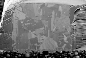
By preventing undercut formation or sidewall etching
High frequency capability
Low roughness etching leads to better SI performance
Ultra-fine
line
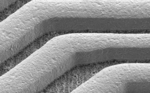
Developed for applications < 8µm L/S, tested successfully down to 1µm L/S
EcoFlash® S300
Our newly developed smart EcoFlash® S300 has overcome most problems of differential etching, by offering a uniform result with a high etch ratio that delivers perfect results with minimal undercutting. This results in higher yields and lower costs.
- High performance differential etch for all SAP, mSAP and ETS applications
- Ideally suited for horizontal conveyorized production
- Chemical regeneration of the oxidizing agent Iron(III) decreases costs and the environmental impact.
- No undercut
- Low roughness for better signal integrity
- Ideal conductor shape
- High etch-ratio
- Minimized line-width reduction
- Chemical regeneration to reduce operating costs
- Broad operating window
What inspires us
Why we developed EcoFlash® S300
Your challenge
As the industry continues to evolve and push the limits of technology, traditional differential etching processes are struggling to keep up with the shrinking line and space sizes. These etching processes are resulting in excessive roughness and/or copper removal at the trace, which fails to meet the stringent requirements of OEMs. In addition, there is a pressing need to increase yield while minimizing operational costs and reducing environmental impact through minimized wastewater expenses.
Our solution
EcoFlash® S300 was developed to address these challenges and enables our clients to stay ahead of the competition in one of the most advanced industries today.
Contact Us