Surface treatment
Integrated wet chemical process and equipment solutions for package substrates and printed circuit boards (HDI/MLB and Flex/Flex-Rigid)
Quick facts
- Global market leader in I/L bonding
- Bespoke solutions for high frequency applications (5G/6G)
- Best in class surface preparation
- Most advanced fine line solutions
- Speciality chemistry designed for the high voltage market
Applications
- PCB / MLB / HDI PCB / Advanced HDI PCB
- Package Substrates
- Flex PCB / Flex-Rigid PCB
- Automotive
Product portfolio
Inner layer bonding enhancement
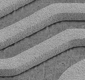
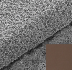
- BondFilm® Part A: Atotech cost-effective and long-time proven oxide alternative process for improved inner layer bonding. With over 400 lines and installations worldwide MKS Atotech leads this market segment globally and contributes to the success of many key PCB manufacturers and OEMs.
- BondFilm® MS 1000: as one of the newest BondFilm® updates, MS 1000 gives great operational benefits, significantly reduce equipment maintenance, sludge formation and downtime frequency.
- BondFilm® HP: our high performing BondFilm® HP reduces sludge to an absolute minimum thus reducing the environmental footprint to a bare minimum while maintaining the excellent performance our BondFilm® series is known for. It is a perfect choice for demanding high voltage applications or solutions where durability play a significant role.
5G / 6G / high frequency applications
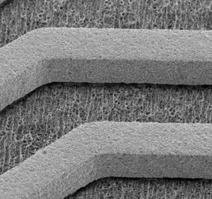
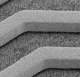
- BondFilm® EX-S2: currently our most advanced oxide replacement for internal layer bonding, specifically designed to combine high frequency capability, reliability and ease of processing. We reduced the roughness requirements, the sludge formation and the environmental impact, to create the perfect tool required for the most sophisticated products.
- NovaBond® EX-S2: we developed NovaBond® EX-S2 especially for demanding IC-substrate applications, where zero line-width reduction, minimum roughening and great adhesion as well as thermal reliability are prerequisites. Our easy four step process ensures up to 40% lower TCOO compared to competitor processes.
- NovaBond® HF2: simple three-step high-frequency adhesion promoter process solution. It is characterized in particular by zero line width reduction and its high compatibility with common high-frequency dielectrics.
Advanced surface preparation
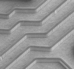
- [Soldermask Pretreatment] CupraEtch® SR 8000: cupric chloride based microetching system with unique additives. The simple three step process creates uniform roughening of surface at low temperatures. Atotech cost-effective pretreatment easily drops into existing lines and reliably improves the adhesion of all copper types to industry standard dryfilm and soldermask types. The metal complex-free solution benefits the cost-effectiveness of waste water treatment.
- [Inkjet Soldermask Pretreatment] InkPromotor T15: anti-bleeding agent for using in combination with a highly controllable cupric chloride-based microetching system CupraEtch® SR 8000. The simple one step process of InkPromotor T15 prevents the capillary action leads to excessive ink flow over the roughened surface, referred to as a BLEED of the ink across the copper surface. It makes ink-jet printing solder mask process with high line resolution possible. As innovative way to produce PCB in an environmentally friendly measure and lower cost.
- [Photoresist Pretreatment] CupraEtch® DF 8000: highly controllable cupric chloride based microetching system with unique additives. The simple three step process creates uniform roughening of surface at low temperatures. Atotech cost-effective pretreatment easily drops into existing lines and reliably improves the adhesion of all copper types to industry standard dryfilm types. The metal complex free solution further contributes to a cost-effective waste water treatment.
- [Differential Etching] EcoFlash® / HyperFlash® Series: innovative one-step process that was developed for differential etching for SAP and MSAP applications with fine line technology.
- [Copper Reduction] HyperEtch® Series: high speed copper removal chemistry, that uniformly trims down the thickness of copper foils, sheets and CCLs.
- [Pretreatment LDD] BondFilm® LDD Series: reliable BondFilm® series has been expanded into the BondFilm® LDD product in order to create a pretreatment and surface that maximizes CO2 laser absorption and ensure improved direct LDD results. This improved laser absorption property yields consistent hole sizes, reduced copper splash than other LDD pretreatments.
- [Posttreatment LDD] BondFilm® LDD SR / LDD Enhancer: copper splash is a negative side effect of all LDD processes. Our BondFilm® LDD SR is especially designed to perfectly remove copper splash with minimal copper removal.
Photoresist stripping
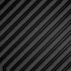
Superior performance of ResistStrip IC for very fine lines
- ResistStrip® Series: extensive range of ResistStrip® Series products ensures that Atotech has the correct solution on offer for every PCB application need. The product range is based on modified hydroxides and amine solutions to guarantee enhanced stripping performance with minimal corrosive attack.
- ResistStrip® IC Series: evolution towards suitability for very fine line production and has been specially formulated to meet the demands of the very demanding IC-Substrate industry. The traditional stripping mechanism has been modified to essentially stop the film swelling that leads to lock in and dry film residues in fine line applications and to perform optimal with advanced manufacturing methods such as SAP.
Metal stripping
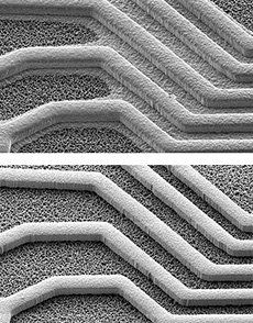
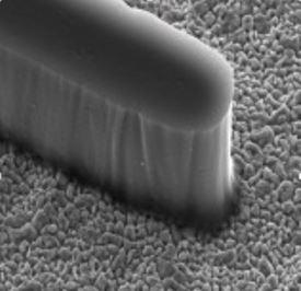
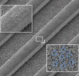
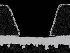
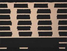
Top: final result without PallaStrip® IC, bottom: final result with PallaStrip® IC
- PallaStrip® IC 2: cyanide free palladium stripper that is suitable for use in removal of palladium containing seed layers. The removal of any seeding layer is critical in fine line applications as they can lead to uncontrolled deposition during subsequent plating operations. PallaStrip® IC 2 offers a simple and easy process solution without the use of any harmful cyanide components, giving the most efficient removal of palladium catalyst deposits with minimal copper removal.
- TinSolv® & SolderStrip®: Atotech range of two-stage and single-stage metal strippers ensure clean and active copper surfaces after metal resist stripping. The formulations of TinSolv® (for tin stripping) and SolderStrip® (for tin / lead removal) enable complete and even stripping, both on the surface as well as in small holes and blind vias.
Direct metal deposition
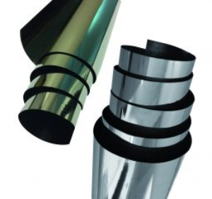
- [MD on Polyimide] CovaBond® Series: enables the creation of fine line and spaces circuitry directly on polyimide films using mSAP and SAP processing technology for high density interconnect (HDI) and chip-on-flex (COF) applications. Compared to the sputter technology Covabond improves the adhesion, reduces the process cost and allows for designs previously not possible.
Plating on glass
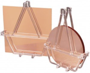
- VitroCoat® GI: an innovative adhesion promoter that enables wet chemical metal deposition on glass. Its competitive advantage is unparalleled metallization coverage in high aspect ratio through-hole vias compared to competing processes such as PVD.
Featured products
BondFilm® HP
High performance adhesion promotor for inner layer bonding
BondFilm® EX-S2
Advanced high frequency adhesion promotor
Novabond® EX
Next generation adhesion promotor for advanced bonding applications
With our newly developed NovaBond® EX process we can offer our customers an innovative and excellent performing solution that provides superior adhesion, consistent peel strength after thermal stress and is highly compatible to a wide range of advanced dielectrics currently used in production, as well as most planned materials in OEM’s future technology roadmaps.
Horizon® BondFilm
Integrated production solution for bonding enhancement and surface treatment technologies
The Horizon® BondFilm system offers ourlatest technology package in chemical processing, thin material conveyance and fluid delivery.
- Horizon® BondFilm LDD – a unique process to improve CO2 laser absorption of surfaces prior to laser direct drilling applications at maximum reliability.
- CupraEtch® – a unique multipurpose micro-etch system for best adhesion of primary imaging resists or solder masks in the production of high quality printed circuits.
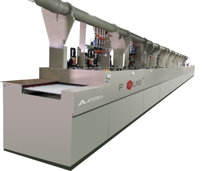
Polygon ST Line ®
Integrated production solution for bonding enhancement and surface treatment technologies
An innovative horizontal system designed for the latest requirements on solder mask and dry film treatment during the production of printed circuit boards.
- Fully compatible with our CupraEtch® process chemistry series and in combination provides a state-of-the-art solutions-based package that combines chemistry, equipment, software and service.
- Optimized for high volume manufacturing, provides maximum yield and best-in-class uniformity over the panel.


