
NovaBond® EX-S2
Ultra low roughness IC Substrate adhesion promotor
Signal transmission
Great SI performance due to ultra low roughness and zero line width reduction
Reliable
Great adhesion performance, thermal reliability and process control
TCOO
The simple four step process reduces the TCOO compared to competitors by 40%
NovaBond® EX-S2
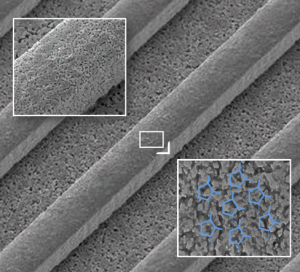
Our high-tech solution for IC substrate inner layer bonding. It combines the advantages of competing processes by applying a brand new innovative technology that ensures high SI performance, thermal reliability and bond strength by creating a nano-roughness in symbiosis with a special patented adhesion molecules, while not affecting the shape of the traces.


NovaBond® EX-S2 has its use as an advanced ahesion promotor for IC Substrate inner layer bonding. It shines where high frequency signal integrity must be preserved.
- Uniform and constant nano-roughening regardless of copper surface type
- High compatibility to various high speed substrate materials
- Preserving conductor shape and size
- Very suitable for ultra fine line application L/S < 5/5 µm
- Signal integrity similar to non-treated: 2% better than low rougness
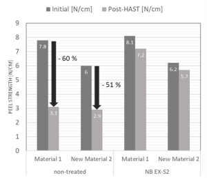
- Great peel strength
What inspires us
Why we developed NovaBond® EX-S2
Your challenge
Ever finer line and spaces are necessary to increase computing power and efficiency. NovaBond® EX-S2 allows for very fine lines that are not negatively affected in terms of line form, width and height.
Our solution
NovaBond® EX-S2 is the most advanced adhesion promotor for IC substrate inner layer bonding. We achieved great adhesion performance and thermal reliability, without altering the dimensions of the conductor traces.