


Thomas Beck
Global Product Director
Semiconductor and Functional Electronic Coatings
Dear readers,
Welcome to the latest edition of our Semiconductor newsletter. In this issue, we present key information on our fan-out packaging for optimal performance in mobile devices and provide you with an insight view on our Semiconductor capabilities in Feucht, Germany. In addition, we would like to introduce you to our new conductor metal for the next technology node interconnects, Atomplate® Cobalt, and our new universal zincation process with our Xenolyte® Conditioner ACA2.
Our article on “Fan-out packaging: a key enabler for optimal performance in mobile devices,” which was published in the Chip Scale Review, provides an overview of our complete portfolio of both chemistry and equipment which we offer in order to address the plating requirements for fan-out.
In our article on Semiconductor Advanced Packaging, we give you an overview of our production capabilities and our commitment to safe, sustainable, and efficient production in our TechCenter in Feucht, Germany. The TechCenter provides a multitude of services, including a clean room environment and a machining production workshop for high precision parts manufacturing.
Our Atomplate® cobalt process is developed in collaboration with Lam Research to provide the necessary cobalt fill of the most advanced feature sizes for the post 7 nm node era. The chemistry is compatible with the extreme demands of this novel integration scheme. The bottom-up fill characteristics of the Atomplate® cobalt process are second to none.
Last but not least, our new universal zincation process with our Xenolyte® Conditioner ACA2 ensures a homogeneous zincate layer for all Al alloys and offers good adhesion for the subsequent Ni layer, thereby overcoming the defects often caused by insufficient zincation. It enables an optimal pretreatment for our subsequent Xenolyte® plating chemistry, which is specified according to Automotive Spec AEC – Q100-010 RE and qualified at many customers of the automotive and power electronics industry.
We sincerely hope that you find this newsletter informative, interesting and useful.
Very best regards,
Thomas Beck
Global Product Director Semiconductor and Functional Electronic Coatings
Publisher: Daniel Schmidt, Head of Electronics Marketing Worldwide
Editor: Yvonne Fütterer, Marketing Specialist Electronics
Please contact us via: Web: atotech.beta.brettinghams-dev.de I Xing: www.xing.com/companies/atotech I LinkedIn: www.linkedin.com/company/atotech
Product highlights
Fan-out packaging – product market fit
“Fan-out packaging: a key enabler for optimal performance in mobile devices,” published January 2017 in the Chip Scale Review

Figure 1: An example FOWLP product-market fit for TSMC’s InFO PoP
Key drivers
The key drivers for the industry to pursue fan-out packaging technologies are 1) better performance, 2) higher I/O density, 3) more functionality, and 4) smaller form factor than flip chip and other WLCSP technologies. The technical benefits of fan-out are 1) better reliability performance by means of embedding and more RDLs; 2) more functionality and higher levels of integration through multi-chip embedding and complex architectures; 3) form factor reduction via innovative architectures; and 4) reduced manufacturing costs with substrate-less embedded technologies. For these reasons, the semiconductor industry will witness the substantial and widespread adoption of FOWLP technologies in the coming years.
Fan-out: exponential growth
Frequently described as a disruptive technology, fan-out will change the packaging landscape with further adoption by outsourced semiconductor assembly and test suppliers (OSATS), integrated device manufacturers (IDMs), and foundries alike. Fan-out packaging, while having recently gained momentum with the entrance of TSMC’s InFO, is not a new technology, however. Embedded wafer-level ball grid array (eWLB) is a type of fan-out packaging that has been in production at Infineon for nearly a decade. Variations of Infineon’s second-generation eWLB technology have been co-developed, qualified, and/or licensed by companies such as STMicroelectronics, STATS ChipPAC, NANIUM S.A., and ASE. Other types of fan-out packages are being produced in low volume at Nepes and Deca Technologies.
TSMC’s entry with its innovative InFO technology has, and will continue to have, a far reaching and lasting impact on the fan-out market. If Apple continues to use InFO PoP technology in future generation iPhones, surely there will be followers. Likewise, Amkor’s recent acquisition of NANIUM, particularly for their FOWLP expertise, further illustrates the significance of FOWLP for next generation packaging and substantiates the claim that fan-out is a strategic technology for those in the mobile supply chain.
In absolute numbers, the growth in fan-out technologies has been quite considerable, increasing from USD 244 million in 2015 to USD 492 million in 2016, and is expected to reach USD 891 million in 2017. According to Yole, the forecast for 2021 is a remarkable USD 1.3 billion with significant growth in both the eWLB and PoP market segments. Market reports by JMS, TechSearch International, and Prismark similarly forecast substantial growth for fan-out packaging.
Fan-out: Cu plating application requirements
The technical advantages and the forecasted market growth position fan-out as the preferred advanced packaging technology for next-generation mobile devices. However, there are still several process challenges associated with fan-out packaging. The following sections discuss requirements for Cu plating applications relative to fan-out packaging technologies.
Requirements for RDL
Trends for next-generation mobile devices – thinner smartphones with more functionality – require miniaturization at all levels. For advanced packaging technologies, miniaturization involves decreasing the RDL pitch down to 2×2µm. Redistribution layers are essential to fan-out technologies, as it is with more RDLs that I/O density is increased. Successful formation and plating of such fine features pose a challenge for both suppliers and manufacturers, with the plating challenge being the simultaneous plating of fine lines, large Cu pads, and microvias for stacked technologies, with a deposition rate that optimizes throughput.
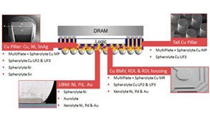
Requirements for Cu pillar
Cu pillars are needed for certain types of fan-out packaging such as package-on package (PoP), in various dimensions including both standard pillar in the range of 40×50µm and tall pillar in the range of 200×50µm. The standard performance requirements – high-throughput, high-yield, and optimal reliability performance – can be met with an optimized Cu pillar process that enables uniform and pure Cu deposition using high-speed plating. High-speed plating will result in a higher throughput, however it also increases the risk of voiding in the intermetallic phase of Cu and SnAg and influences uniformity, both of which impact the electrical performance and yield. The purity of the deposit, and specifically the presence of organic co-deposition, also influences the voiding performance. Therefore, a good Cu pillar process should enable high-speed plating of pure and uniform Cu. This can be achieved with the right organic additives and high-speed plating equipment that collectively reduce the occurrence of organic co-deposition and optimize uniformity. When electroplating tall Cu pillars, the situation is more complex, as it is more challenging to plate high aspect ratio structures in a timely manner. (Further details about our tall pillar process are available in the Chip Scale Review article.)
You can find the full article here.
To address the plating requirements for fan-out, Atotech offers a complete portfolio of both chemistry and equipment, and is currently working on innovative solutions to tackle next-generation challenges.
- Spherolyte Cu MPX, together with our MultiPlate® system, enables extremely fast plating of pure, uniform, and thick Cu. This process has demonstrated best in class performance in terms of plating speed, non-uniformity, and organic co-deposition on wafers from leading foundries and OSATs.
- Spherolyte Cu UF5 process for next generation packaging, currently in R&D, will enable perfectly flat and very pure Cu deposits at ≥20 ASD. Atotech’s synthesized molecule and method for this process is one-of-a-kind, and will enable technical benefits that positively and significantly impact reliability performance and throughput.
- Spherolyte Cu UF3 RDL process is designed for both fine line plating and microvia filling for 3D stacked technologies. This process produces stable and optimal mechanical properties within a wide process window and at high purity levels. The use of high purity chemistries reduces the risk of microvoids that amass after thermal cycle testing and lead to breakages in the Cu metal lines.
- Spherolyte Cu UF3 pillar process is market leading in terms of purity and eliminates the need for a Ni diffusion barrier before soldering, thereby reducing process steps and time, and increasing throughput. This process enables pure and uniform Cu depositions at higher current densities than industry standard ASDs.
- Spherolyte Cu UF2 process enables very high speed plating with optimal non-uniformity.
- Spherolyte Ni and Spherolyte Sn ECD processes for Cu pillar capping.
- Various electroless processes – Xenolyte Ni, Xenolyte Pd, and Xenolyte Au – are available for pad metallization and the housing of RDL structures for oxidation prevention and adhesion promotion.

For more information, please contact:
Cassandra Melvin
Global Product Manager
Semiconductor and Functional Electronic Coatings
Atotech Deutschland GmbH
Phone: +49 (0)30 – 349 85445
E-mail: cassandra.melvin@atotech.com
Product highlights
Semiconductor Advanced Packaging – What are our competencies?
Equipment production in cleanroom environment for next generation technologies
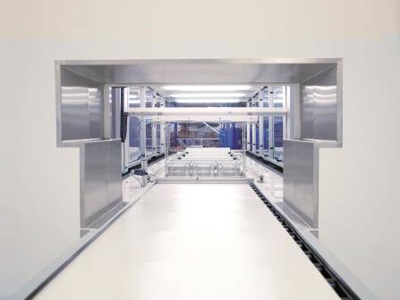 Figure 1: Clean Room production in Feucht
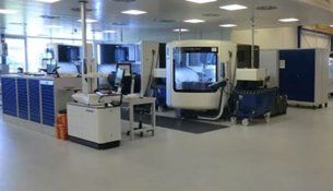 Figure 2: CNC machines for parts manufacturing
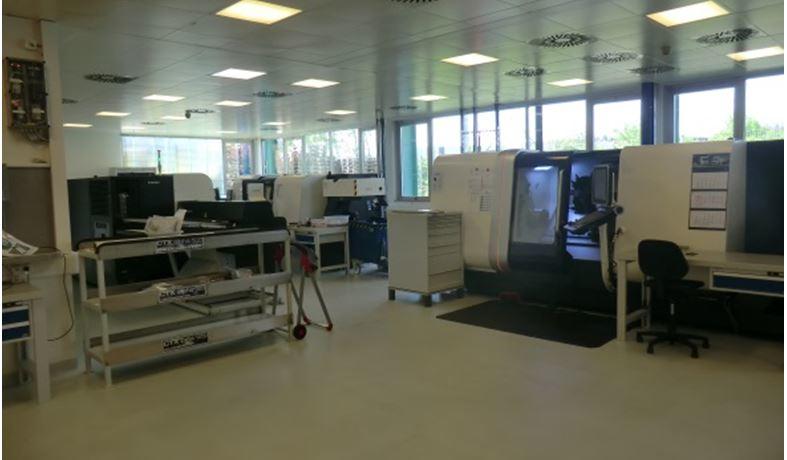 Figure 3: CNC machines for parts manufacturing
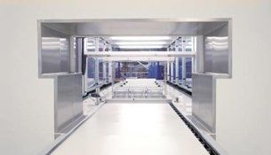
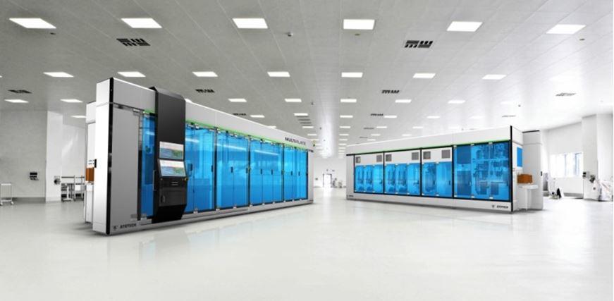 Figure 4: Final assembly area in an ISO8/ISO7 clean room environment with MultiPlate® equipment
Our unique network of TechCenters offers a variety of services in all of our main business areas. At the heart of our semiconductor R&D activities as well as our cleanroom equipment production are our facilities in Europe, specifically in Feucht, Germany.
Semiconductor equipment production
Our complete, state of the art equipment clean room production facility is located in Feucht. The 2,000 m² clean room was built in 2012 and meets ISO 8/7 standards. Equipment manufactured in our cleanroom facility is specially designed to satisfy the high cleanliness standards and requirements for fine line capability, while enabling very high speed plating of next generation technology features.
The cleanroom production site is used for the manufacturing of our MultiPlate® platform for wafer-level and panel-level packaging and Semiconductor applications as well as for the assembly of our VisioPlate® platform, which allows the metallization of up to G8 glass panels for the display manufacturing industry.
Machining production workshop for high precision parts manufacturing
Our production in Feucht features a high precision and highly automated CNC parts manufacturing production workshop. This accommodates our leading semiconductor machining equipment and is being used for the production of parts in a clean environment. The production area offers different high tech production machines with high speed milling, five axis milling and combined lathe/milling machines. All CNC machines produce leading precision parts and components via integration with Atotech’s CAM system.
MultiPlate® equipment
Our MultiPlate® equipment is also manufactured at our clean room manufacturing site in Feucht. MultiPlate®, an innovative ECD plating system, is designed to meet the current plating market requirements and the challenges of emerging technologies in advanced packaging. Together with our high purity Spherolyte® chemistries, MultiPlate® allows for simultaneous front and backside plating with optional individual process control for each side of the substrate and is designed for high volume manufacturing of both round wafer and square panel substrates. Additional system features provide technical benefits for embedded technologies – such as better heat management and energy efficiency –. MultiPlate® can be customized according to individual production requirements and enables the further miniaturization of power semiconductor packages to comply with future product requirements.
Sustainable production
As environmental regulations become more rigorous, we remain committed to our core values and the development of innovative and sustainable technologies that enable our customers to improve process efficiency and minimize their environmental footprint.
During production of semiconductor equipment, materials like plastic, PVC, stainless steel, etc. are recycled and a heat recovery system is employed for 70% energy regeneration in our cleanroom equipment production area.
In addition to employing sustainable manufacturing methods, we strive to develop products that are sustainable and processes that are energy efficient. We continue to monitor environmental regulations and adjust our products accordingly. We also heavily invest in R&D for next generation technologies, with the goal to provide products that are free of CMR, toxic, and allergenic substances, as well as heavy metals. Our lead free nickel and cyanide free gold for pad metallization are two examples of products that exemplify Atotech’s commitment to the elimination of dangerous and toxic substances.
- Controlled temperature and humidity
- Regular particle measuring and tracking
- Line testing with high purity DI water
- Spray cleaning of incoming parts / Ultrasonic cleaning of small parts
- Sit-over bench in entrance lock incoming parts
- Clean room class: ISO8/ISO7
- Area: 2,000m²
- Airflow: 33,000m²/h
- Air exchange: 12x/h
- Heat recovery: 70%
For more information, please contact:
Felix Schmidt
Manager Business Development Equipment worldwide
Atotech Deutschland GmbH
Phone: +49 (0)912 872-5633
E-mail: Felix.schmidt@atotech.com
Product highlights
Atomplate® Cobalt – A new conductor metal for the next technology node interconnects
Electrolytic cobalt enables continued scaling for contact level interconnects

Figure 1: Logarithmic comparison of resistance/length vs wire cross-sectional area total across metal splits as calculated using temperature-dependent resistance and TEM metrology. (from Chawla et al, AMC/IITC 2016[1])
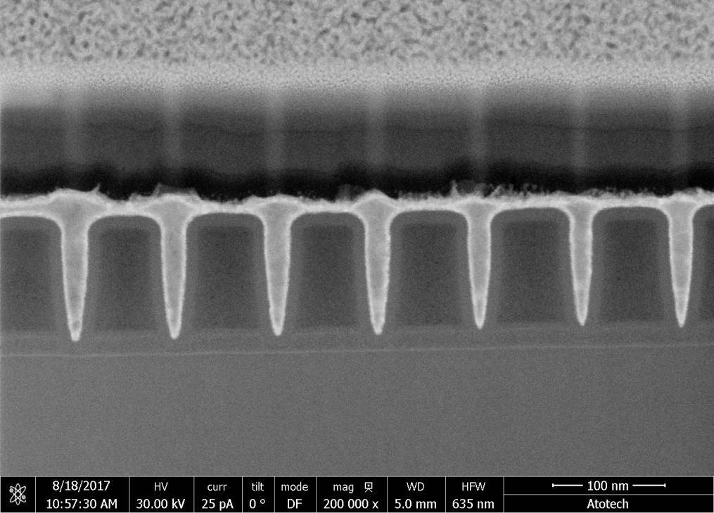
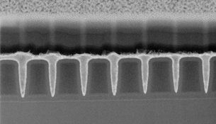
Figure 2: STEM micrograph of sub 20 nm interconnect features filled with the Atomplate ECD cobalt process.
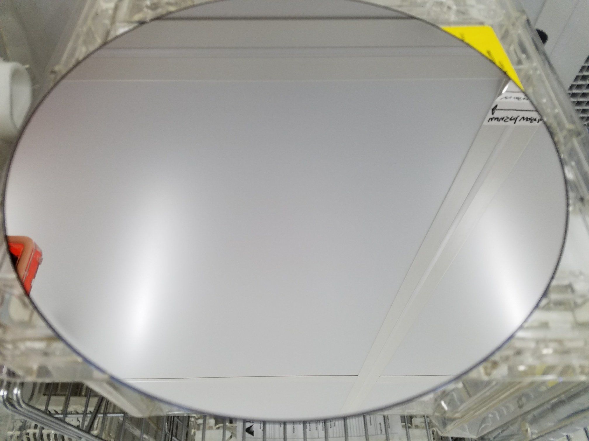
Figure 3: Blanket wafer plated on a Lam Research Sabre ECD tool. The film shows no observable defects.

Figure 4: Fill of patterned areas on a wafer showing planar overburden over dense small features and a minor dimple over large pads. Complete planarization over large dimension features can be achieved by using a secondary additive.
For wire cross-sectional areas below 100 nm2, electron interface scattering plays a dominant role in the effective conductor resistivity; and subsequently wiring resistance becomes unacceptably high. Compared to traditional interconnect metals such as copper for the back end of the line (BEOL) damascene interconnects and tungsten for contact level interconnects, low electron mean free path metals can bring a benefit in wiring resistance for wire diameters below 100 nm2. The use of these metals allows some additional freedom in interconnect dimension scaling as resistivity values remain tolerable and scale more linearly with dimensions than the traditional metals.
Novel contact level interconnect metals
Candidates for novel contact level interconnect metals are cobalt, ruthenium and rhodium. Rhodium has not been considered due to cost, as well as limitations in familiarity in the traditional integration schemes. Ruthenium has been evaluated by N. Jourdan et all (e.g. AMC/IITC 2016 [2]) however process cost and challenges in the integration scheme for chemical vapor deposition (CVD) or atomic layer deposition (ALD) filled contact features limit the benefit of using this metal. Additionally, as a ruthenium bottom-up type filling process does not exist, seam voiding impacts overall usefulness of this metal as a replacement for tungsten.
Of the three listed metals, cobalt has been the preferred choice; integration schemes with cobalt as a conductor metal offer an advantage in contact resistance as well as conductor resistivity. These properties of cobalt ensure scalability beyond 5 nm node technologies. Cobalt has also been around in both front-end as well as back-end of the line integration schemes for quite a while. CVD cobalt in particular has seen use in contact silicide, interconnect liners and interconnect capping metals. Integration schemes using CVD cobalt in combination with a reflow and a subsequent PVD cobalt film have been evaluated as a process for filling the contact level interconnects. Despite adequate electrical and reliability results, a two-tiered deposition process has not readily been accepted due to cost and process time considerations. Additionally, the inherent non-planarity of vapor deposition processes over larger interconnect features has proven to be hard to handle for chemical mechanical planarization (CMP) techniques.
ECD cobalt – the preferred choice
ECD cobalt is a major contender to fulfill the role, in part due to the low cost of the process, but more so due to its capability to provide true bottom-up cobalt filling of even the smallest contact level interconnects. Bottom-up fill can be achieved with low-complexity base electrolytes, largely compatible with industry standard plating tools. The plating process works well with a TiN/CVD Co barrier/seed integration scheme, and void free fill shows a fill profile exceeding the quality of the well-known damascene copper process. Pre-CMP planarity requirements can be met by adjusting bath and plating parameters.
Atotech’s Atomplate® cobalt process
The Atomplate® cobalt process is developed in collaboration with Lam Research to provide the necessary cobalt fill of the most advanced feature sizes for the post 7 nm node era. Designed for exclusive use on the Lam Research Sabre ECD Cu platforms, this chemistry is compatible with the extreme demands of this novel integration scheme. The bottom-up fill characteristics of the Atomplate® cobalt process are second to none; features with openings below 20 nm can be filled without pinch off, seams, or interface voids (see Figure 2). Planarity and film quality requirements can be met with ease by plating parameter adjustment (see Figures 3 and 4), or by the use of a secondary additive.
References:
[1] Resistance and Electromigration Performance of 6 nm Wires, J.S. Chawla et al. IEEE AMC/IITC, May 2016 [2] CVD-Mn/CVD-Ru-based Barrier/Liner Solution for Advanced BEOL Cu/Low-k Interconnects, N. Jourdan et al, IEEE AMC/IITC, May 2016
- Promotes a void free fill through a true bottom up cobalt fill process
- Compatible with ultrathin CVD Co seed, TaN and TiN barrier
- Adjustable mounding and planarity control for a variety of features by hardware controls
- Provides high purity, low resistivity cobalt films (< 100 ppm C, O, Cl, N total, S-free)
- Provides highly reflective, low in-film defect count films
- Optimization of overburden and film quality is possible through secondary bath additive
- Compatible with standard cobalt base electrolytes

For more information, please contact:
Jobert van Eisden, Ph.D.
Director Dual Damascene and Semiconductor Applications Engineering
Atotech Semiconductor Technology
Phone: +1-518-894-3080
E-mail: Jobert.van-eisden@atotech.com
Product highlights
Xenolyte® Conditioner ACA 2- a new universal zincation for pad metallization in power electronics industry
Universal Al pretreatment as key enabler for reliable electroless Ni, Pd and Au Pad metallization
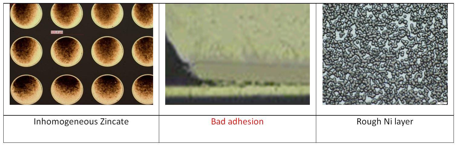
Figure 1: Defects of insufficient Zincation
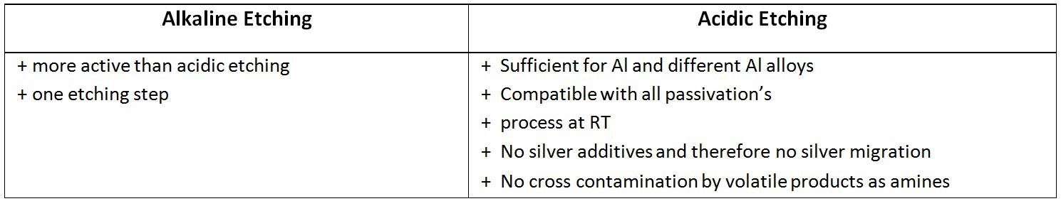
Figure 2: Advantages of alkaline and acidic Al oxide etching

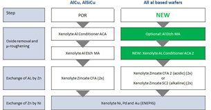
Figure 3: Process sequence of standard zincation and new modified universal zincation
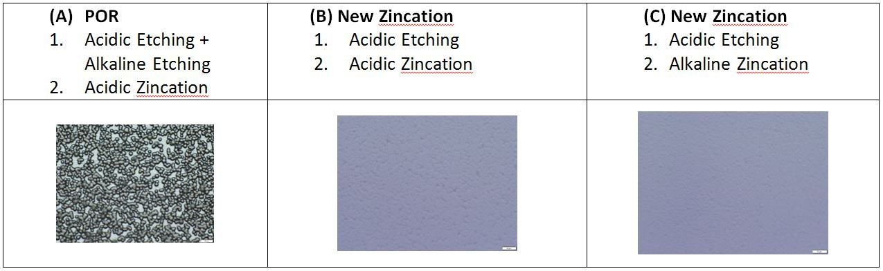
Figure 4: Comparison of Ni layer after standard POR zincation and new universal zincation process
Despite the advantages of emerging technologies, such as embedding, reliable wire bonding and soldering are still the dominant packaging technologies in the automotive industry. Both technologies require under bump metallization (UBM) to meet high package reliability requirements. Pad/Under Bump Metallization is used to protect the underlying interconnects, improve adhesion and provide a robust and stable interconnection of bond pads for soldering and wire bonding. Apart from Cu, most of the bond pads typically consist of sputtered Al and Al alloys, such as Al, AlCu, AlSi and AlSiCu.
The zincation process
Out of various UBM processes the electroless deposition of Ni, (Pd) and Au (EN(EP)IG) on bond pads has proven to be a promising technology to fulfil technical and economic advantages. Before the ENEPIG process can be applied, though, it is necessary to prepare the surface and remove the Al oxide layer which is formed immediately when Al pads are exposed to oxygen.
This so called zincation process contains a cleaning step to remove oxide layers and a zincate step to prevent re-oxidation, activate the surface and enable a proper adhesion for the following Ni deposition. Preferably, the zincate formation step is applied twice (double zincation) to ensure a smooth and homogeneous deposit as well as improved adhesion of the UBM stack on the Al.
Since the industry uses a variety of different Al and Al alloys, different pretreatment conditions are required in terms of time, temperature and pH to overcome defects caused by insufficient zincation (see figure 1).
The main root causes of these defects are:
- Insufficient removal of Al passivation The insufficient removal of the Al oxide prohibits the zincate formation and results in an inhomogeneous zincate layer. In addition, the residues of Al oxide decrease the adhesion of the subsequent Ni layer and lead to seam formation, which can later on be attacked by corrosion after the Au deposition.
- Uneven and over etching of Al As the thickness and bonding strength of Al oxide and Al varies based on the Al grain orientation, the oxide removal during etching can be uneven and attack the pure Al locally.
In general, the Al oxide layer can be removed by an acidic or alkaline etching step with benefits towards acidic etching as listed in figure 2. The main advantage of an acidic etching step is that it is compatible with polyimide which is often used as resist or passivation.
New universal zincation process with Xenolyte® Conditioner ACA 2
In comparison to our standard zincation POR, which is limited to AlCu and AlSiCu surfaces, our new universal zincation process ensures a homogeneous zincate layer for all Al alloys and offers good adhesion for the subsequent Ni layer. It was therefore necessary to modify the sequence of the acidic etching step and develop a new conditioner – Xenolyte® Conditioner ACA 2. Figure 3 shows the differences between our new universal zincation process and our standard POR. The new acidic etching process can also be combined with an alkaline or acidic zincate formation step.
Figure 4 shows the Ni plating results of standard zincation compared to our new universal zincation process. The standard zincation shows a non-closed, rough Nickel layer (A) whereas the new zincation shows a regular and closed Ni deposit (B). Especially for the zincation of Al and AlSi alloys, further optimizations could be achieved by combining acidic etching and alkaline zincate deposition (C).
The new universal zincation process, using our Xenolyte® Conditioner ACA 2, expands our electroless UBM portfolio to treat all Al alloys and delivers a reliable pretreatment. It enables an optimal pretreatment for our subsequent Xenolyte® plating chemistry, which is specified according to Automotive Spec AEC – Q100-010 RE and qualified at many customers of the automotive and power electronics industry.
For more information, please contact:
Markus Hoerburger
Assistant Product Manager Semiconductor and Functional Electronic Coatings
Atotech Deutschland GmbH
Phone: +49 (0)30 – 349 851669
E-mail:markus.hoerburger@atotech.com
Trade show news
Global events and trade shows
Figure 1: ASMC 2017

Figure 2: SEMICON China

Figure 3: Uwe Hauf, CTO at Atotech Deutschland GmbH, at the Lucky Draw at ISS 2017
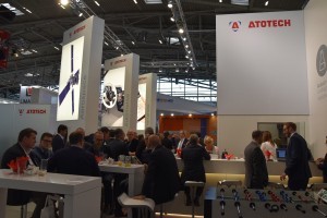 Figure 4: Atotech’s booth at the productronica / SEMICON Europa 2017
This year, the Advanced Semiconductor Manufacturing Conference (ASMC) was held from May 15 to 18, 2017, in Saratoga Springs, New York, USA. As the leading international technical conference for exploring solutions to improve the collective micro-electronics manufacturing expertise, the ASMC had record visitors in 2017.
Atotech was among the presenting companies at the ASMC 2017. Titled “Simultaneous front and back side Cu metallization on power chips,” the poster presentation outlined the many advantages of our Multiplate® equipment, such as the pure, low stressed deposit of Cu and a fast and highly efficient process flow.
SEMICON China 2017
As one of the most influential and premier gatherings for semiconductor professionals SEMICON China 2017, which took place from March 14 to 16, 2017, in Shanghai, China, was attended by more than 69,000 visitors. The range of interests was accordingly broad, spanning over a range of industries, technologies, and products from across the supply chain, and from design to final manufacturing.
Visitors could meet with Atotech’s experts and specialists at its booth no 5363 to discuss latest technology roadmaps, product developments, and key solutions such as MultiPlate® – a versatile and innovative ECD packaging tool -, Xenolyte® Zincate CFA2 – a universal pretreatment process for all types of Al and Al alloy wafers – or Spherolyte® RDL/Pillar 3 – a copper pillar plating process enabling flat and recess free pillar plating -.
ISS 2017
The SEMI Industry Strategy Symposium (ISS) Europe took place from March 5 to 7, 2017, in Munich, Germany. The Symposium gathers prominent experts from around the world to define future market demands and customer requirements. It provides practical insight into the applications now driving the developments of the industry, and addresses fundamental technology developments of the future and what this will mean for the markets and industries served.
Atotech was the official sponsor of the “Lucky Draw” at the ISS Europe 2017, with Uwe Hauf, Chief Technology Officer at Atotech Deutschland GmbH, presenting one lucky visitor of the draw with an iPad Air.
SEMICON Europa 2017
This year’s SEMICON Europa was co-located with productronica at the Messe Munich in Munich, Germany, and took place from November 14 to 17, 2017. While Hall B1 was dedicated to SEMICON Europa, Halls B2 and B3 featured productronica. This unique co-located event created the strongest single event for electronics manufacturing in Europe. The high turnout also demonstrates the growing importance of business networking and global cross-collaboration, supporting SEMIs mantra of “Connect, Collaborate, and Innovate.”
Atotech participated with two presentations at SEMICON Europa:
- On Wednesday, November 15th, Andreas Walter, Team Manager Electroless Processes Semiconductor Advanced Packaging at Atotech Deutschland GmbH, presented “Direct electroless under bump metallization (UBM) for wire bonding and soldering on next generation power semiconductor materials”
- On Thursday, November 16th, Thomas Beck, Business Director Semiconductor Advanced Packaging at Atotech Deutschland GmbH, presented “Additive impact on Cu microstructure for sub 10µm L/S”
Furthermore, Cassandra Melvin, Global Product Manager Semiconductor Advanced Packaging at Atotech Deutschland GmbH, functioned as Session Chair at the PE Conference, Session 4 on “Integration and packaging of power devices and outlook”, on Wednesday, November 13, from 10:00 to 11:00 am!
Meet our experts and senior leaders at key global events coming up around the world:
SEMICON Korea 2018
Date: January 31 – February 02, 2018
Venue: COEX, Seoul, Korea
ISS Europe 2018
Date: March 04 – 06, 2018
Venue: Clontarf Castle Hotel, Dublin, Ireland

Industry News
Market and technology
At a glance report of all the important market and technology News you can’t miss.

Samsung will invest USD18.6 billion to widen lead in memory market
Samsung will extend its lead in memory chips and next generation smartphone displays, by heavily investing in new capacity and infrastructure in South Korea. The investment will create nearly half a million jobs, with an expected 440,000 new roles by 2021.
Source: http://uk.reuters.com/article/uk-samsung-elec-chips-idUKKBN19P05D
Qualcomm turns to TSMC for 7nm node production of Snapdragon 845
Qualcomm has ended partnership with Samsung for manufacturing of next generation Snapdragon chipset. Current chips are 10 nm node technology and next gen 7 nm node processors will be manufactured by TSMC and called Snapdragon 845.
Source: http://vr-zone.com/articles/qualcomm-ditches-samsung-sides-tsmc-7nm-snapdragon-845/127575.html
Korea replaces Taiwan as the largest semiconductor equipment market
Korea surpassed Taiwan in Q1/2017, with billings at US$3.53 billion, rising 48% on quarter and 110% from a year earlier. Meanwhile equipment billings in Taiwan fell 16% sequentially but increased 84% on year to USD 3.48 billion.
Source: http://www.digitimes.com/pda/a20170606PR203.html
200 mm fab investment finds home in China
China is hugely investing in wafer fab capacity (over a dozen new 300 mm fab announcements in the past few months) while at the same time launching more new 200 mm fab projects and capacity additions than any other region. China currently has about 700,000 wafers per month (wpm) installed fab capacity. This is forecasted to surpass 900,000 wpm by the end of 2021. By then, China’s 200 mm capacity is expected to surpass America, Japan, and Taiwan, and be second only to Europe.
Source: http://www.semi.org/en/200mm-fab-investment-finds-home-china-0
Challenges for future Fan-Outs
The fan-out wafer-level packaging market is heating up. Several packaging houses are developing new fan-out packages that could reach a new milestone and hit or break the magic 1µm line/space barrier. The article in the Semiconductor Engineering highlights the challenges the technology faces as well as current packaging trends and possible solutions the various industry players pursue.
Source: http://semiengineering.com/challenges-future-fan/
Bosch announced to build new 300mm fab in Dresden
Robert Bosch GmbH will invest USD 1.1 billion in a new semiconductor fab in Dresden, Germany. The construction will be completed end of 2019 and the first operation is scheduled for early 2021. The new fab will address the growing demand in IoT and mobility applications.“By extending our semiconductor manufacturing capacity, we are giving ourselves a sound basis for the future competiveness”, Volkmar Denner, Chairman of the Board of Management of Robert Bosch GmbH, mentioned.
Source: http://www.bosch-presse.de/pressportal/de/en/new-bosch-wafer-fab-in-dresden-germany-111360.html
Foxconn Invests USD 10 billion in U.S. LCDs – Ambitious bid to create “8K+5G” ecosystems
Hon Hai Precision, the parent company of Foxconn, will spend USD 10 billion to build in Kenosha, Wisconsin a 10.5-generation LCD plant for 8K displays. The deal brokered by the Trump Administration includes USD 3 billion in tax breaks to create at least 3,000 Foxconn jobs in the U.S. “[…] this is part of a bigger plan to create a robust 8K+5G ecosystem in the United States,” Gou said, Foxconn Chairman and founder.
Source: http://www.eetimes.com/document.asp?doc_id=1332072&