
Printoganth® MV TP2
Next Generation Electroless Copper for Fine Line SAP Applications
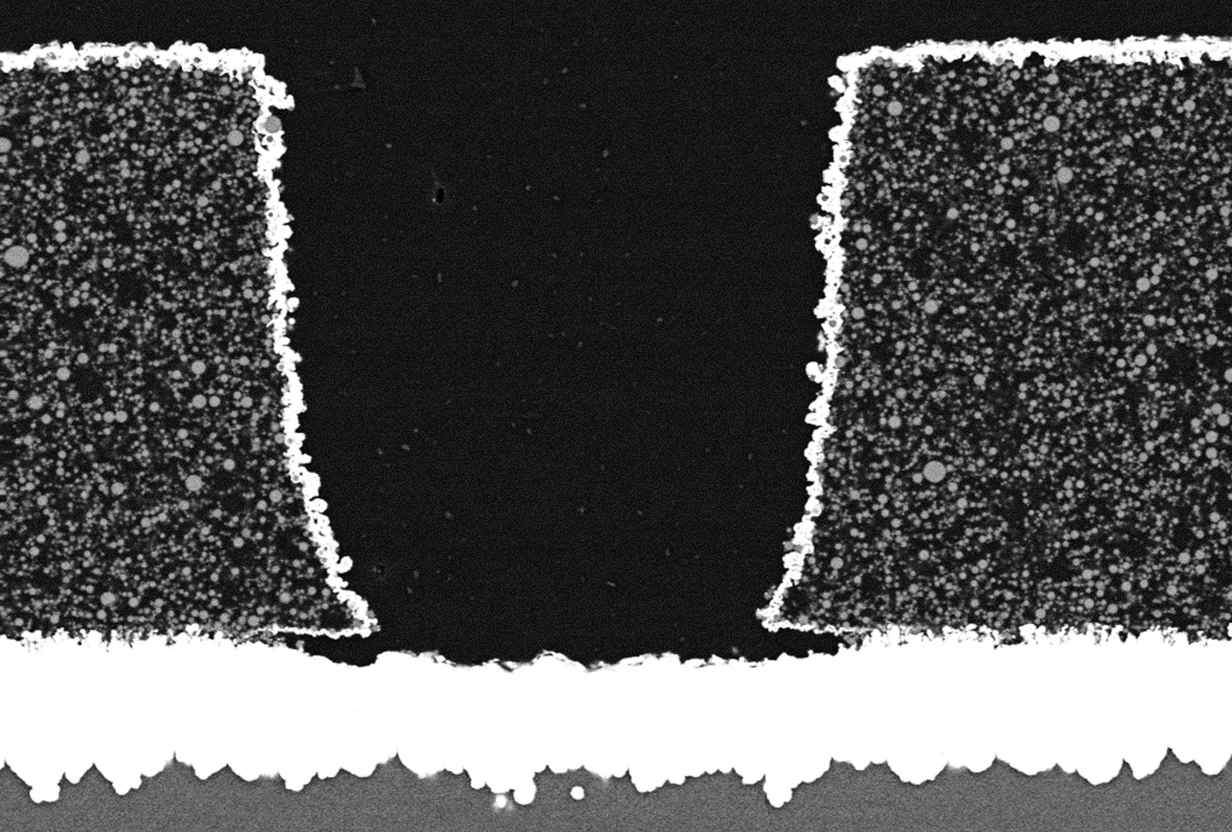
Excellent throwing power
Consistently achieved in BMVs with challenging dimensions
Production ready – Fast
Quick bath initiation with low dummy plating
Mixed production capability
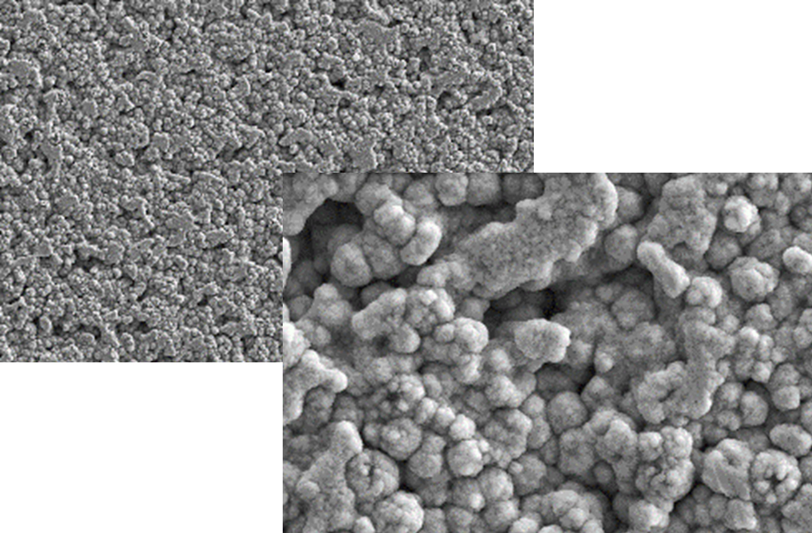
Low deposition thickness supports fine line & high frequency applications

- High-end IC substrates based on SAP technology
- IC substrates using amSAP technology
- Ideal for mixed production facilities targeting SAP with amSAP
- Excellent throwing power into challenging BMVs
- Reduced process costs due to low dummy plating
- Low bath initiation: 0.2 dm² c.b./L for 10min
- Bath loading factor: ≥ 0.1 dm² c.b./L/li>
- Thin deposit (0.25 μm) with controlled levelling characteristics supports fine line & high frequency applications/li>
- Stabilizer analysis available for improved process control/L/li>
What inspires us
Why we developed Printoganth® MV TP2
Your challenge
The next generation of IC substrates require finer line and spaces features than existing designs, and in order to achieve this, surface Copper thickness must be minimized. Contradictorily, the Copper thickness within micro vias has to be maximized to ensure coverage for subsequent pattern plating operations. In addition, “high frequency” applications require a uniform deposit thickness with optimal roughness to enhance dry film adhesion, which is also critical for fine line SAP manufacturers.
Our solution
Printoganth® MV TP2 is Atotech’s most upto date solution for meeting the miniaturization requirements that are cascading down from the semiconductor arena, and into the high-end IC Substrate market. Printoganth® MV TP2 offers superior throwing power performance, with a low deposition thickness that opens up the next stage in feature size reduction.
With an optimized deposit structure, Printoganth MV TP2 creates a uniform textured Copper layer that is ideal for low loss applications and enhanced dry film adhesion.